Active production — no lifecycle risk for this NPN RF transistor
The BFU710F,115: RoHS3 compliant, with no restricted substances above the threshold — no exemption expiry to track.
43 GHz fT and noise figure — where this transistor fits the signal chain
The BFU710F,115 is an NPN silicon RF transistor with a 43 GHz transition frequency. That fT places it comfortably above the 5.8–12 GHz band where the noise figure is specified — 0.85 dB typ at 5.8 GHz, 1.45 dB typ at 12 GHz. The transistor has enough gain margin at those frequencies that the noise figure, not the fT, sets the LNA cascade budget. Maximum collector current is 10 mA, with a 2.8 V collector-emitter breakdown. The 136 mW power dissipation limits the bias point — for a typical LNA biased at 2 V and 5 mA, the 10 mW dissipation leaves plenty of headroom below the 150 °C junction limit. DC current gain (hFE) is a minimum of 200 at 1 mA, 2 V, confirming the transistor is in the flat-beta region at typical LNA bias currents.
SOT-343F package — footprint and handling
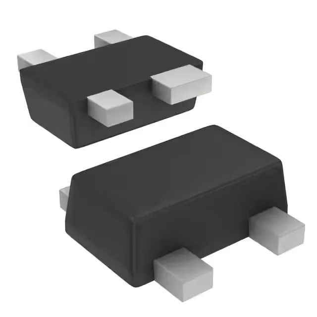
Housed in a SOT-343F package, also designated 4-DFP. This is a 4-lead surface-mount plastic package with a collector pad on the back side — the ground plane under the package is part of the RF layout, not just a thermal path. Supplied on Tape & Reel or Cut Tape. Surface-mount only; no through-hole variant exists in the series.