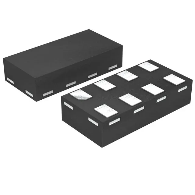
NXP Semiconductors 74HC3GU04GD,125 — Analog & Data Acquisition
Technical Documents PDF / CAD
RoHS Compliant · Lead-Free EIA-481 Standard
NXP Semiconductors / Analog & Data Acquisition

NXP 74HC3GU04GD,125 Triple Inverter, 2V-6V, 8-XSON

MPN 74HC3GU04GD,125
End of Life Spot Stock · 24-48h Dispatch 100% Original Sealed

NXP Semiconductors 74HC series, Logic Type Inverter, 3 Circuits, 3 Inputs, 2V ~ 6V Supply, -40°C ~ 125°C, Surface Mount, 8-XFDFN Package, 74HC3GU04GD,125.

In Stock: 50,455 pcs
MOQ: 1 pcs
Logistics: DHL / FedEx DAP (Global Express · 3-7d) Russia & CIS DDP (Door-to-Door Cleared)
Dispatch: Shenzhen / HK
Unit Price (USD)
$0.17 / pc
Direct Purchase Ready
Volume Pricing Breaks Confirmed upon quotation
1+ pcs
$0.17
10+ pcs
$0.15
30+ pcs
$0.14
100+ pcs
$0.13
500+ pcs
$0.12
1,000+ pcs
$0.11
Working on a production BOM or have a target unit price? Submit Target Price
Buy Now

$0.17 / ea

50,455 in stock — maximum per order · 3–4 days lead time

$0.15 / ea from 10 pcs

Upload Full BOM List
[SPEC] Essential Parameters Snapshot Full Specifications (14)
Package / Case 8-XFDFN
Supply Voltage 2V ~ 6V
Output / Current 5.2mA, 5.2mA

Full Technical Specifications

14 Parameters
74HC3GU04GD,125 specifications
Parameter / AttributeSpecification / Value
Series74HC
Logic typeInverter
MountingSurface Mount
Supply voltage2V ~ 6V
Current - quiescent20 µA
Current - output high, low5.2mA, 5.2mA
I/O channels3
Operating temperature-40°C ~ 125°C
PackageBulk
Case8-XFDFN
Number of circuits3
Input logic level - low0.5V ~ 1.8V
Input logic level - high1.5V ~ 4.2V
Max propagation delay @ v, max CL5ns @ 6V, 50pF
Series Sibling Variants

NXP Semiconductors 74HC Series Models

Sibling variants, package options, and speed/density grades in this NXP Semiconductors semiconductor series. Active Shenzhen warehouse allocation and rapid 24-48h dispatch.

Technical Details & Description

Triple unbuffered inverter — 74HC logic, 2V to 6V rail

The NXP 74HC3GU04GD,125 is a triple unbuffered inverter in the 74HC family, providing three independent inverting gates with a single input each.

Switching speed and drive — 5 ns at 6V, 5.2 mA per output

Maximum propagation delay is 5 ns at 6V supply with a 50 pF load — the timing budget for a 20 MHz clock tree or a fast data path stays tight. The 5.2 mA output drive (both high and low) is enough to switch a downstream CMOS gate or drive a short PCB trace without a buffer. Quiescent current maxes at 20 µA — negligible for a battery-powered sensor node that spends most of its time in a static logic state. The input logic thresholds scale with supply: low at 0.5V to 1.8V, high at 1.5V to 4.2V, so the inverter triggers cleanly on standard 3.3V or 5V logic levels.

Package and board-fit — 8-XSON (2x3 mm), 0.5 mm pitch

Surface-mount assembly with MSL (Moisture Sensitivity Level) per JEDEC — the 8-XSON package is typically MSL 1, but verify the reel date code for bake requirements before reflow. The narrow 0.5 mm pitch demands a solder paste inspection step to catch bridging between adjacent pins.

Active production — sourcing and compliance

No official second-source or pin-compatible alternative is listed for this exact order code. The 74HC family includes other triple-gate variants (e.g., 74HC3G04 for buffered output), but the unbuffered topology of the 3GU04GD means the output slew rate is not shaped — a consideration for signal-integrity-sensitive traces.

Frequently asked questions

What is the propagation delay of 74HC3GU04GD,125?

Maximum propagation delay is 5 ns at 6V supply with a 50 pF load. At lower supply voltages the delay increases — budget 10-12 ns at 3.3V for timing closure.

What compliance documentation does NXP provide for 74HC3GU04GD,125?

The part is ROHS3 compliant. NXP provides a material declaration and REACH compliance data on request; no UL or IEC certification is listed for this logic device.

74HC3GU04GD,125
Verified Allocation
Quote