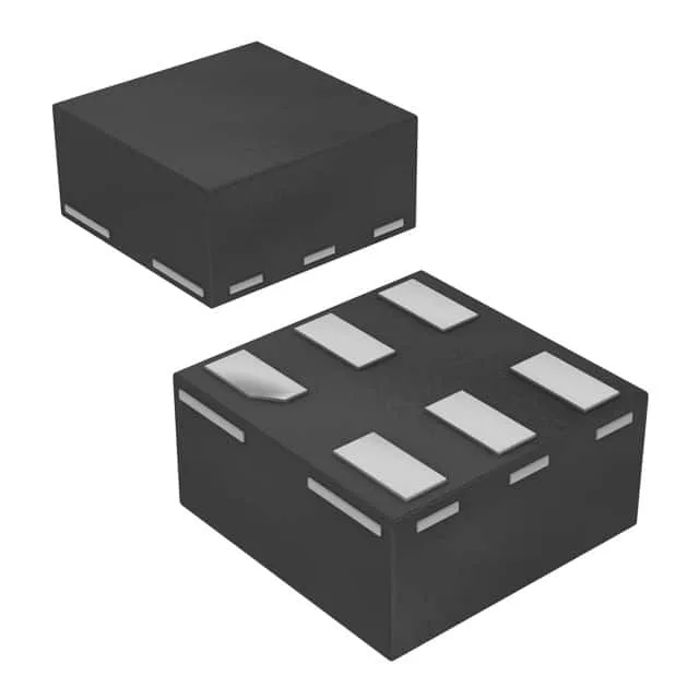
Single OR gate for ultra-low-power and space-constrained designs
The Nexperia 74AUP1G32GF,132 is a single 2-input OR gate from the 74AUP ultra-low-power CMOS logic family. It operates from a supply voltage range of 0.8V to 3.6V, making it suitable for multi-voltage battery-powered systems where a single logic gate must bridge different power domains without external level shifters. The maximum quiescent current is just 500 nA, which is critical for always-on blocks in wearables, IoT sensors, and portable medical devices where every microamp extends battery life. Propagation delay is 6.4 ns at 3.3V with a 30 pF load, fast enough for most low-to-mid-speed glue logic tasks.
The 0.8V to 3.6V supply range means it can be powered directly from a 1.2V or 1.8V rail in low-voltage SoC designs, or from a standard 3.3V rail in legacy systems, without needing a separate regulator. Input logic levels are specified as low at 0.7V to 0.9V and high at 1.6V to 2V, ensuring compatibility with both 1.8V and 3.3V logic families.
Output drive and speed
The gate can source or sink 4 mA of output current, sufficient to drive a single standard CMOS load or a short PCB trace. The 6.4 ns propagation delay at 3.3V is typical for this power-optimized family; if faster switching is required, a 74LVC or 74AHC series gate would be a better fit, though at higher quiescent current. For most low-frequency control signals, clock enables, or reset distribution, the 74AUP1G32GF,132 provides ample margin.