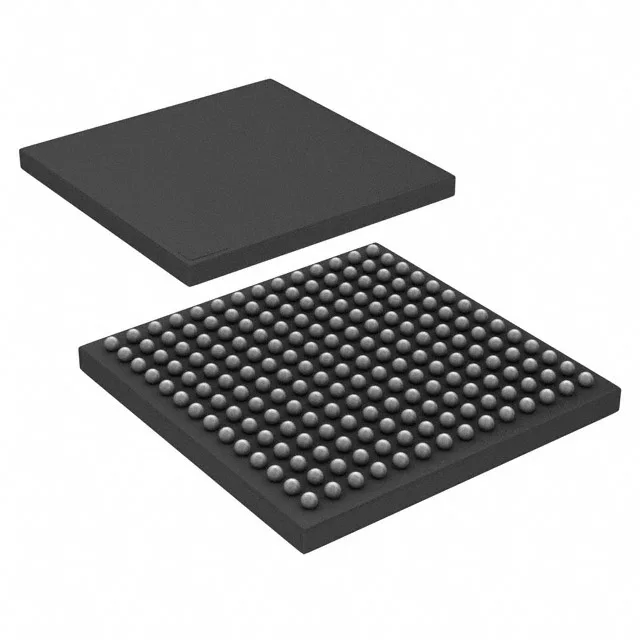
The NXP MIMXRT1052DVJ6B is a crossover MCU from the RT1050 series, built around a single ARM Cortex-M7 core clocked at 600 MHz. It carries 512K x 8 of on-chip RAM and executes code from external Flash or SDRAM — no internal program memory, so the boot media choice (parallel NOR, HyperFlash, or serial NAND) drives the PCB layout. The 196-LFBGA package (12x12 mm) keeps the footprint compact but demands a multi-layer PCB with via-in-pad capability for the BGA balls. Operating temperature is 0°C to 95°C junction — commercial grade, so it belongs in indoor equipment, not under-hood or outdoor enclosures.
The 600 MHz core speed enables real-time control loops and TCP/IP stacks simultaneously. The 3V–3.6V supply rail needs adequate decoupling for transient loads.
Memory architecture — external program memory only
This MCU has no internal Flash for program storage. Code executes from external memory — typically a parallel NOR Flash, HyperFlash, or Quad-SPI serial NOR, accessed through the FlexSPI controller. The 512K x 8 on-chip SRAM is used for data, stack, and cache. That means the BOM must include a Flash device plus a voltage regulator for the 3V–3.6V core supply. The external memory interface (EBI/EMI) also supports SDRAM for larger data buffers. Plan the PCB stack-up to route the FlexSPI signals with controlled impedance and matched length for reliable operation at the 600 MHz core speed.