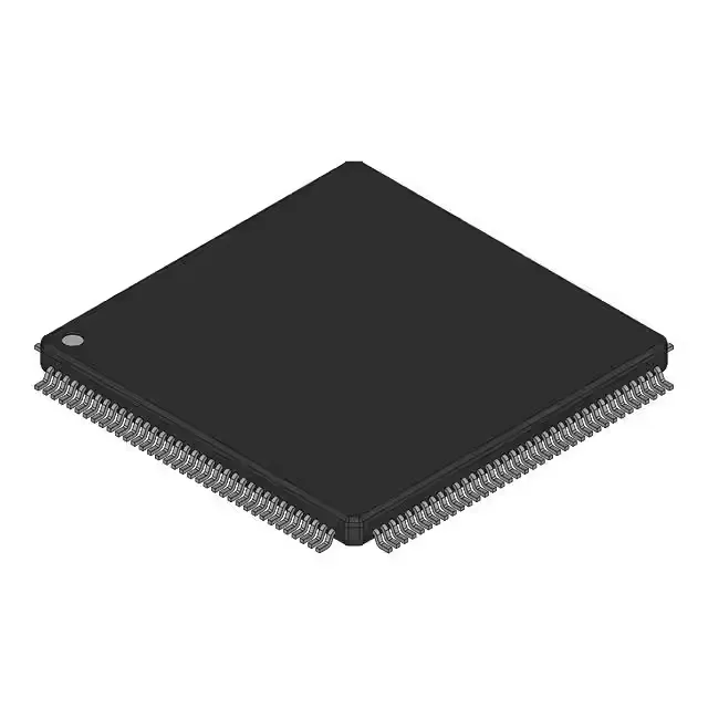
NXP USA Inc. LPC18S10FBD144551 — Microcontrollers & Processors (MCU / MPU / DSP)

NXP LPC18S10FBD144551 MCU, ARM Cortex-M3, 180 MHz, 144-LQFP

MPNLPC18S10FBD144551
Active

NXP LPC18S10FBD144551, LPC18xx series, 32-bit ARM Cortex-M3 single-core at 180 MHz, ROMless external-flash architecture, 2.2–3.6 V supply, 144-LQFP (20×20 mm), 83 I/O, CANbus, 8×10b ADC, 1×10b DAC, DMA, SD/MMC, -40°C to 85°C, Active.

$7.1200Ref. price · indicative, final on quote
Packaging144-LQFP
SeriesLPC18xx
Independent supplier — new & surplus stockAuthenticity-screened · ESD-safe packingListing updated Jul 2026

Specifications

LPC18S10FBD144551 specifications
ParameterValue
SeriesLPC18xx
MountingSurface Mount
Oscillator typeInternal
Program memory typeROMless
Voltage - supply (Vcc (Vdd))2.2V ~ 3.6V
Operating temperature-40°C~85°C(TA)
Speed180MHz
PackageBulk
RAM size136K x 8
Core size32-Bit Single-Core
PeripheralsBrown-out Detect/Reset, DMA, I²S, POR, PWM, WDT
ConnectivityCANbus, EBI/EMI, I²C, IrDA, Microwire, MMC/SD, SPI, SSI, SSP, UART/USART
Number of i (O)83
Core processorARM® Cortex®-M3
Case144-LQFP
Data convertersA/D 8x10b; D/A 1x10b

Product details

180 MHz Cortex-M3 with ROMless external-flash architecture

The ROMless architecture means all code executes from external Flash or SRAM via the EBI/EMI interface — a deliberate choice for systems where firmware size exceeds internal Flash limits or where the memory map must be shared with an FPGA or application processor. The 136K x 8 of on-chip RAM handles data buffers and stack; the rest of the memory budget is on the board.

CANbus and industrial connectivity

The peripheral set also includes I²C, SPI, SSI, SSP, UART/USART, IrDA, Microwire, MMC/SD, and EBI/EMI — enough serial and parallel bandwidth to bridge a CAN bus to a local display, an SD card logger, or a sensor array. The 83 general-purpose I/O lines leave room for local control and status monitoring without an external GPIO expander.

Frequently asked questions

Does LPC18S10FBD144551 have internal flash or require an external memory?

The LPC18S10FBD144551 is ROMless — it has no internal Flash for program storage. All code must reside in external memory (NOR Flash, SRAM, or SDRAM) accessed through the EBI/EMI interface. The on-chip 136K x 8 RAM is for data only.

Is LPC18S10FBD144551 suitable for CAN bus applications?

Yes, the LPC18S10FBD144551 includes a CANbus interface in its connectivity set, making it suitable for CAN-based industrial control, automotive auxiliary nodes, and building automation gateways.

What is the LPC18S10FBD144551 pinout and is it compatible with other LPC18xx devices?

The LPC18S10FBD144551 uses the standard 144-LQFP (20×20 mm) pinout shared across the LPC18xx family. It is pin-compatible with other LPC18xx MCUs in the same 144-LQFP package, so a board designed for an LPC1857FBD144 can accept this ROMless variant without layout changes — only the external memory configuration differs.

What is the recommended replacement or equivalent for LPC18S10FBD144551?

Within the LPC18xx family, the LPC1857FBD144 is a common Flash-based sibling that shares the same 144-LQFP footprint and peripheral set. The key difference is that the LPC1857 includes on-chip Flash, while the LPC18S10 is ROMless. If your design already uses external memory, the LPC18S10 is the correct choice; if you want to eliminate the external Flash, the LPC1857 is the pin-compatible alternative.

What is LPC18S10FBD144551's listed speed?

The core runs at 180 MHz, which is the maximum clock for the ARM Cortex-M3 on this device.