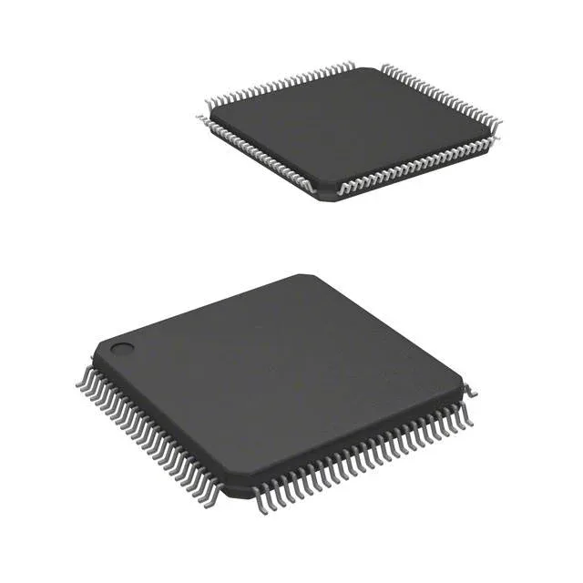
NXP USA Inc. LPC1766FBD100K — Microcontrollers & Processors (MCU / MPU / DSP)

NXP LPC1766FBD100K — 100MHz Cortex-M3 MCU, 256KB Flash, 100-LQFP

MPNLPC1766FBD100K
Active

NXP LPC17xx series ARM Cortex-M3 MCU, order code LPC1766FBD100K; 100MHz clock, 256KB Flash, 64KB SRAM; 70 I/O, Ethernet, USB OTG, CAN, SPI/I²C/USART; 2.4–3.6V single rail; -40°C–85°C; 100-LQFP (14×14mm) surface-mount package.

$16.2300Ref. price · indicative, final on quote
Packaging100-LQFP
StockContact for availability
MOQ1 pcs
  • 100% new & originalTraceable channels only — no refurbs, no pulls, no remarked parts.
  • Date & lot codes on quoteStated per line before you commit; label photos on request.
  • MSL-compliant ESD packingMoisture-sealed bags with indicator cards; reels photo-verified.
  • PayPal buyer protectionPay by T/T, PayPal or Payoneer — card payments covered end to end.

Specifications

LPC1766FBD100K Technical Specifications
ParameterValue
SeriesLPC17xx
Mounting typeSurface Mount
Oscillator typeInternal
Program memory typeFLASH
Voltage - supply (Vcc (Vdd))2.4V ~ 3.6V
Operating temperature-40°C~85°C(TA)
Speed100MHz
PackageBulk
RAM size64K x 8
Core size32-Bit Single-Core
PeripheralsBrown-out Detect/Reset, DMA, I²S, Motor Control PWM, POR, PWM, WDT
ConnectivityCANbus, Ethernet, I²C, IrDA, Microwire, SPI, SSI, UART/USART, USB OTG
Number of i (O)70
Core processorARM® Cortex®-M3
Case100-LQFP
Data convertersA/D 8x12b; D/A 1x10b
Program memory size256KB (256K x 8)

Frequently asked questions

Is the LPC1766FBD100K still active or has NXP moved it to discontinued?

Active, ROHS3 compliant. No last-time-buy or PCN flag is present in the current record.

Is there a drop-in compatible or second-source MCU with the same 100-LQFP footprint and flash density?

The same-function sibling in the LPC17xx family with a higher flash density is the LPC1768 — it shares the 100-LQFP package, 100MHz Cortex-M3 core, and 70-I/O footprint but doubles the Flash to 512KB, giving headroom for firmware images that approach the 256KB ceiling on the LPC1766. If the design requires a pin-compatible alternate with more memory, the LPC1768 is the validated family cross-reference. No officially designated second-source alternate outside the NXP LPC17xx family is present in the current record.

Does the 64KB SRAM allow simultaneous TCP/IP stack, USB OTG buffers, and motor control PWM table in one firmware image?

The 64KB SRAM figure is on-chip. Whether it accommodates simultaneous TCP/IP stack, USB OTG DMA buffers, and motor control PWM lookup tables depends on the firmware footprint and which RTOS or bare-metal allocator is used — the silicon provides the resource; the firmware engineer allocates it. Designs approaching the SRAM ceiling should confirm their stack/buffer sizing against the 64KB figure before BOM lock.