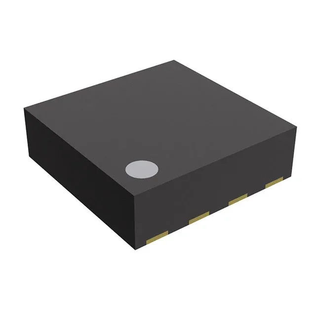
Fixed 3.3V at up to 800 mA — what the rating drives
The RP402K331A-TR is a synchronous step-up regulator delivering a fixed 3.3 V rail at up to 800 mA from a 0.6–4.8 V input range. The 800 mA ceiling is most constrained at the low end of the input window — at 0.6 V in and 3.3 V out the duty-cycle headroom is tight, so the actual achievable load current drops before you reach that limit. Verify your V_IN minimum against the load requirement before committing to the BOM line.
Why synchronous rectification matters at 1.2 MHz
Built-in synchronous rectification replaces the external catch diode found in a conventional boost converter — that diode accounts for the bulk of efficiency loss in non-synchronous designs. Combined with the 1.2 MHz switching frequency, the converter achieves high efficiency in a compact footprint because the external inductor can be smaller. The 1.2 MHz clock also keeps switching noise above the typical audio band, reducing input filtering requirements in noise-sensitive analog sections.
Single-cell battery compatibility and the 0.6 V input floor
The 0.6 V minimum input is the distinguishing spec for this part — it lets the regulator start and regulate from a single NiMH or alkaline cell that is already partially discharged, below the voltage where a non-boost rail would drop out. This makes it suited for portable or battery-backed equipment where the rail must stay up as the battery depletes, not just at full charge.
Thermal path through the exposed pad
The 8-pin count keeps the pinout simple for a boost regulator: VIN, VOUT, GND, and a handful of control pins — confirm pin functions against the manufacturer datasheet before laying out the footprint.
Operating temperature and industrial-grade ambient
For a enclosed chassis or a board adjacent to a dissipating processor, derate the output current further than the 800 mA headline to stay within the junction temperature limit. The package type Tape & Reel or Cut Tape is the standard reel format for pick-and-place assembly.