What the 20 ns and 8 macrocells mean for your logic
The GAL16V8-20LVC is an electrically-erasable PLD from the GAL®16V8 family, packing 8 macrocells with a 20 ns propagation delay. That 20 ns figure sets the maximum clock rate — with registered outputs, the device can reliably clock at up to 50 MHz, assuming the external routing and output loading stay within the datasheet derating curves. The 8 macrocells give you enough logic to replace a handful of 74-series TTL or CMOS glue-logic parts on a single chip. The EE PLD programmability means you can erase and reprogram the device electrically — no UV eraser needed. This is useful during prototyping when the logic equations change a few times before they lock.
20-PLCC footprint and surface-mount assembly
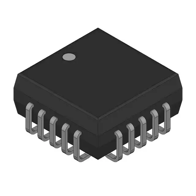
Housed in a 20-lead PLCC (J-Lead) package, the GAL16V8-20LVC measures 8.89 mm square. The J-lead footprint is common in 1990s-era programmable logic designs and still available in many socketed or soldered applications. Surface-mount assembly is standard — the PLCC body sits flush against the board, with the leads folded under. For hand-assembly or low-volume runs, Bulk is fine.
Active lifecycle and compliance note
One important flag: the GAL16V8-20LVC is marked RoHS non-compliant. If your BOM requires full RoHS 5/6 or RoHS 3 exemption-free compliance, this part does not meet that requirement. For legacy designs or projects with a RoHS exemption, it remains a valid choice.