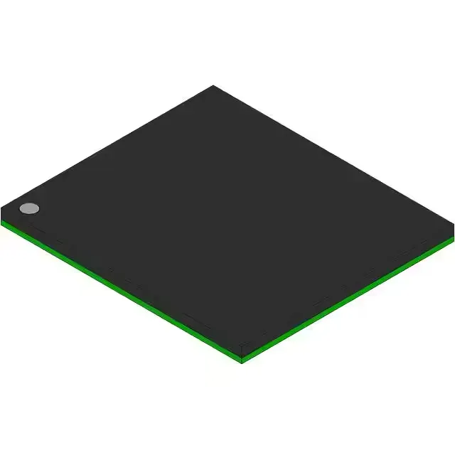
Micron Technology MT55L256L18P1F-10 — Memory (DRAM / SRAM / Flash / EEPROM)
Technical Documents PDF / CAD
RoHS Compliant · Lead-Free EIA-481 Standard
Micron Technology / Memory (DRAM / SRAM / Flash / EEPROM)

Micron MT55L256L18P1F-10 ZBT SRAM, 4Mbit, 5 ns, 100 MHz

MPN MT55L256L18P1F-10
End of Life Spot Stock · 24-48h Dispatch 100% Original Sealed

Micron ZBT® SRAM, MT55L256L18P1F-10, 4Mbit (256K x 18), 5 ns access time, 100 MHz clock, parallel interface, 3.135V–3.465V supply, 0°C to 70°C, 165-FBGA (13x15 mm).

In Stock: 149 pcs
MOQ: 1 pcs
Logistics: DHL / FedEx DAP (Global Express · 3-7d) Russia & CIS DDP (Door-to-Door Cleared)
Dispatch: Shenzhen / HK
Unit Price (USD)
$5.51 / pc
Direct Purchase Ready
Volume Pricing Breaks Confirmed upon quotation
1+ pcs
$5.51
10+ pcs
$4.96
30+ pcs
$4.52
100+ pcs
$4.08
Working on a production BOM or have a target unit price? Submit Target Price
Buy Now

$5.51 / ea

149 in stock — maximum per order · 3–4 days lead time

$4.96 / ea from 10 pcs

Upload Full BOM List
[SPEC] Essential Parameters Snapshot Full Specifications (14)
Package / Case 165-TBGA
Supply Voltage 3.135V ~ 3.465V
Speed / Frequency 100 MHz
Memory / RAM 4Mbit

Full Technical Specifications

14 Parameters
MT55L256L18P1F-10 specifications
Parameter / AttributeSpecification / Value
SeriesZBT®
Memory typeVolatile
MountingSurface Mount
Supply voltage3.135V ~ 3.465V
Clock frequency100 MHz
Memory interfaceParallel
Operating temperature0°C ~ 70°C (TA)
PackageBulk
TechnologySRAM - ZBT
Access time5 ns
Memory size4Mbit
Memory formatSRAM
Case165-TBGA
Memory organization256K x 18
Series Sibling Variants

Micron Technology ZBT® Series Models

Sibling variants, package options, and speed/density grades in this Micron Technology semiconductor series. Active Shenzhen warehouse allocation and rapid 24-48h dispatch.

Technical Details & Description

The Micron MT55L256L18P1F-10 is a 4 Mbit ZBT (Zero Bus Turnaround) synchronous SRAM organized as 256K x 18 bits. It is designed for high-throughput applications where back-to-back read and write cycles must occur without dead cycles — think packet buffers in network switches, cache in telecom line cards, or look-up tables in FPGA-based accelerators. The 5 ns access time and 100 MHz clock rate let it keep pace with a 100 MHz bus without wait states, so timing closure on a high-speed memory interface is straightforward.

Package and mounting — 165-ball FBGA

It is surface-mount only — no socket option.

For volume BOM commitments, an RFQ is the right next step.

Frequently asked questions

Is MT55L256L18P1F-10 obsolete or end-of-life?

No, the MT55L256L18P1F-10 is listed as Active in production. There is no end-of-life notice or last-time-buy window currently in effect.

What is the access time of MT55L256L18P1F-10?

The access time is 5 ns, which allows single-cycle read/write at the rated 100 MHz clock.

Is MT55L256L18P1F-10 RoHS compliant?

No, the MT55L256L18P1F-10 is listed as RoHS non-compliant. Check your assembly house's exemption policy if lead-free solder is required.

What is the exact package and pinout of MT55L256L18P1F-10?

The package is a 165-ball TBGA (13x15 mm body), surface-mount only. The pinout is defined by the Micron ZBT SRAM family standard; consult the device datasheet for the ball-map diagram.

Does MT55L256L18P1F-10 require any special programming or configuration?

No special programming is required. It is a standard synchronous SRAM with a parallel interface; configuration is handled entirely by the memory controller at power-up.

MT55L256L18P1F-10
Verified Allocation
Quote