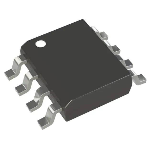
Microchip Technology TC4425AVOA — Power Management (PMIC / Gate Driver)

TC4425AVOA Low-Side Gate Driver, 4.5A Peak, 8-SOIC

MPNTC4425AVOA
End of Life

Microchip TC4425AVOA, low-side gate driver, dual independent channels, 4.5A peak source/sink, 12ns rise/fall, 4.5V to 18V supply, -40°C to 150°C junction, 8-SOIC package.

$2.24Ref. price · indicative, final on quote
Packaging8-SOIC (0.154", 3.90mm Width)
RoHSROHS3 Compliant
Independent supplier — new & surplus stockAuthenticity-screened · ESD-safe packingListing updated Aug 2026

Specifications

TC4425AVOA specifications
ParameterValue
Gate typeN-Channel, P-Channel MOSFET
Input typeInverting, Non-Inverting
Channel typeIndependent
MountingSurface Mount
Voltage4.5V ~ 18V
Logic voltage - VIL, VIH0.8V, 2.4V
Current - peak output (Source, sink)4.5A, 4.5A
Operating temperature-40°C ~ 150°C (TJ)
PackageTube
Case8-SOIC (0.154\", 3.90mm Width)
Number of drivers2
Driven configurationLow-Side
Rise (Fall time)12ns, 12ns

Product details

Dual 4.5A low-side driver with inverting and non-inverting inputs

The Microchip TC4425AVOA is a dual-channel low-side MOSFET driver that delivers 4.5A peak source and 4.5A peak sink current per channel, with typical rise and fall times of 12ns into a 2500 pF load. Each channel accepts both inverting and non-inverting input signals, so a single part handles N-channel and P-channel MOSFET gate drive without external logic inverters. The supply range spans 4.5V to 18V, covering 5V logic rails through 12V and 15V gate drive levels.

150°C junction rating — thermal headroom for tight enclosures

The 150°C TJ ceiling gives the designer extra margin when the driver sits near hot MOSFETs or inductors on a dense board.

12ns edges — fast enough for 500 kHz switching, layout matters

The 12ns rise and fall times (typical at 2500 pF load) enable efficient switching up into the hundreds of kilohertz. Those fast edges reduce cross-conduction losses in the driven MOSFET but also demand a low-inductance layout — the gate-drive loop from driver output to MOSFET gate and back to the driver ground should be kept under 1 cm. The 8-SOIC package (0.154-inch body width, 3.90 mm) is a common footprint that fits existing PCB layouts for dual low-side drivers.

Frequently asked questions

What is the peak output current of TC4425AVOA?

The TC4425AVOA delivers 4.5A peak source and 4.5A peak sink current per channel, specified at the driver output. This is the peak capability into a capacitive gate load; the actual current delivered depends on the gate charge and the driver's internal resistance.

Is TC4425AVOA compatible with 5V logic?

Yes. The logic input thresholds are 0.8V (VIL) and 2.4V (VIH), so the driver accepts 3.3V and 5V logic levels directly. The supply voltage can be as low as 4.5V, allowing the driver to run from a 5V rail while still driving the gate to the full rail voltage.

Is TC4425AVOA RoHS compliant?

Yes, the TC4425AVOA is ROHS3 compliant.