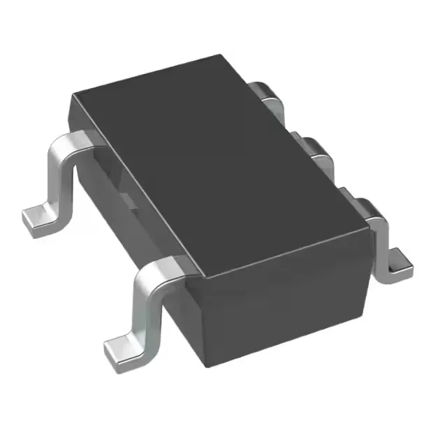
Package and board-fit for rework
The TC1185-5.0VCT713 comes in a SOT-23-5 package (SC-74A, SOT-753), five pins with a 0.95 mm pitch — easy to hand-solder or hot-air rework without lifting pads. The Enable pin on pin 3 gives you a clean shutdown without pulling the input rail. Surface-mount only, so plan the board layout for the small footprint; the thermal pad is the die attach, not an exposed paddle, so the SOT-23-5 relies on copper pour and via stitching under the package to keep junction temperature in check at full 150 mA load.
Output spec and what it means for the rail
Fixed 5 V output at up to 150 mA — this is a clean rail for powering analog front-ends, MCU I/O banks, or sensor bias supplies that need better regulation than a switcher's ripple. The 0.4 V max dropout at 150 mA means the input must stay above 5.4 V to hold regulation at full load; below that the output follows the input minus dropout. Quiescent current is 80 µA typical — low enough for battery-powered gear that spends most of its time in sleep, though not as aggressive as the sub-µA LDOs in the same class. The Enable pin lets you cut that to near zero when the rail is not needed. For an ADC reference or precision op-amp supply, that is the difference between a clean conversion and noise coupling into the signal chain.
Temperature range and protection for industrial use
The over-current and over-temperature protection mean the part shuts itself down before the die cracks under a sustained short or a hot reflow cycle.