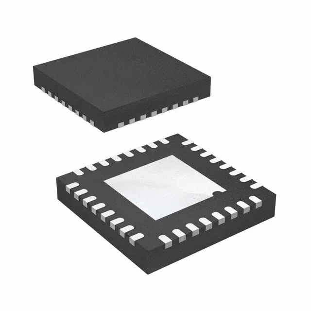
Microchip Technology SY75578LMG — Clock & Timing ICs

Microchip SY75578LMG Clock Buffer, 2:8 Fanout, 267 MHz

MPNSY75578LMG
End of Life

Microchip Technology Precision Edge® clock buffer, SY75578LMG, 2:8 fanout, 267 MHz max, HCSL output, 32-VFQFN exposed pad, tube.

$4.94Ref. price · indicative, final on quote
Packaging32-VFQFN Exposed Pad
RoHSROHS3 Compliant
SeriesPrecision Edge®
Independent supplier — new & surplus stockAuthenticity-screened · ESD-safe packingListing updated Aug 2026

Specifications

SY75578LMG specifications
ParameterValue
SeriesPrecision Edge®
MountingSurface Mount
Voltage3.135V ~ 3.465V
Frequency267MHz
Operating temperature-40°C ~ 85°C
PLLNo
InputHCSL, LVDS
OutputHCSL
PackageTube
Main purposePCI Express (PCIe)
Case32-VFQFN Exposed Pad
Number of circuits1
Ratio - Input:Output2:8
Differential - Input:OutputNo/Yes

Product details

2:8 fanout at 267 MHz — PCIe clock distribution without PLL jitter

The SY75578LMG is a 2:8 fanout clock buffer from Microchip's Precision Edge® family, designed to distribute a PCIe reference clock without adding PLL-induced jitter — there is no internal PLL, so the output jitter tracks the input source. It accepts HCSL or LVDS inputs and outputs eight HCSL copies at up to 267 MHz, covering PCIe Gen1 (100 MHz), Gen2 (100 MHz), and Gen3 (100 MHz) base clock rates with margin. The differential input-to-output path is transparent — the input is AC-coupled, and the output is HCSL with a controlled swing that meets the PCIe reference clock specification without external termination resistors.

Industrial temperature range and supply tolerance

The supply range is 3.135 V to 3.465 V — a 3.3 V nominal rail with ±5 % tolerance stays inside this window, but a 3.0 V rail does not; the board must regulate to 3.3 V. Single-circuit design (one buffer channel) with a 2:8 input-to-output ratio means two independent clock inputs each fan out to four outputs, or one input fans out to all eight when the second input is unused.

32-QFN with exposed pad — thermal and layout notes

Packaged in a 32-VFQFN with exposed pad, 5x5 mm body. The pad also serves as the low-inductance return path for the HCSL outputs — a poor ground connection raises output jitter above the datasheet limit.

Frequently asked questions

What is SY75578LMG's input and output type?

It accepts HCSL or LVDS inputs and outputs HCSL only. The input-to-output path is differential with no PLL, so the output signal is a buffered copy of the input.

What PCIe generations does the 267 MHz maximum frequency support?

267 MHz covers PCIe Gen1, Gen2, and Gen3 base clock rates (all 100 MHz) with margin. Gen4 and Gen5 require a higher-frequency buffer.

What compliance documentation does Microchip provide for SY75578LMG?

The part is ROHS3 compliant. Microchip provides a datasheet with electrical characteristics, thermal data, and application notes. No UL or IEC certification is listed for this device.