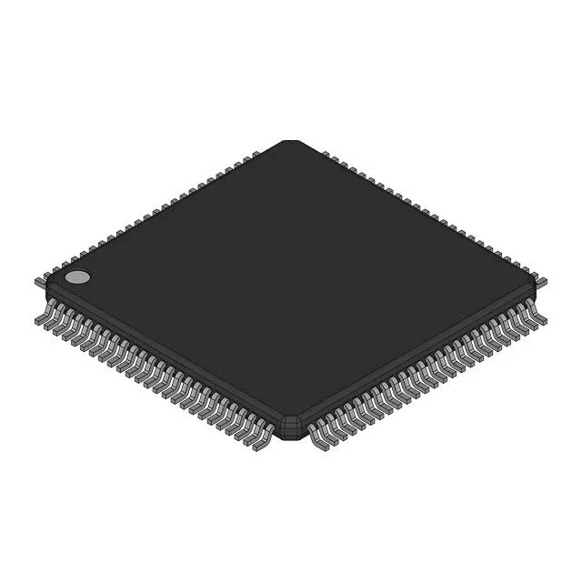
Lattice Semiconductor OR2T04A4T100I-DB — FPGA / CPLD & Programmable Logic

Lattice OR2T04A4T100I-DB FPGA, 160 I/O, 6400 bits RAM

MPNOR2T04A4T100I-DB
Active

Lattice Semiconductor ORCA™2 FPGA, OR2T04A4T100I-DB, 160 I/O, 6400 total RAM bits, 11000 gates, 400 logic elements, 3 V supply, -40°C to 85°C, Surface Mount, Bulk.

$11.56Ref. price · indicative, final on quote
Independent supplier — new & surplus stockAuthenticity-screened · ESD-safe packingListing updated Aug 2026

Specifications

OR2T04A4T100I-DB specifications
ParameterValue
SeriesORCA™2
MountingSurface Mount
Operating temperature high-40°C to 85°C (TJ)
Package_typeBulk
Number of i (O)160
Total ram bits6400
StatusActive
Number of gates11000
Supply voltage3.0
Number of logic elements (Cells)400

Product details

ORCA™2 FPGA — 160 I/O and 6400 RAM bits

The Lattice Semiconductor OR2T04A4T100I-DB is an ORCA™2 family FPGA delivering 160 user I/O, 6400 total RAM bits, and 11000 gates in a Surface Mount package. With 400 logic elements (100 CLBs) and a 3 V supply rail, this part targets combinatorial and registered logic integration where the I/O count and on-chip memory budget are the binding constraints.

Industrial temperature grade and supply

The 3 V nominal supply (3.3 V typical for the ORCA2 family) means the core and I/O banks share a single rail — no separate VCCIO regulator needed for 3.3 V interfaces.

Frequently asked questions

What is the OR2T04A4T100I-DB's on-chip memory and logic capacity?

It provides 6400 total RAM bits, 11000 gates, and 400 logic elements (100 CLBs) — enough for glue-logic integration and small state machines without external SRAM.

Does the OR2T04A4T100I-DB replace the LCMXO2-256HC-4MG132I?

No — the LCMXO2-256HC-4MG132I is a different family (MachXO2) with 55 I/O and 256 logic elements; the OR2T04A4T100I-DB has 160 I/O and 400 logic cells, so a direct drop-in is not possible without a board spin.