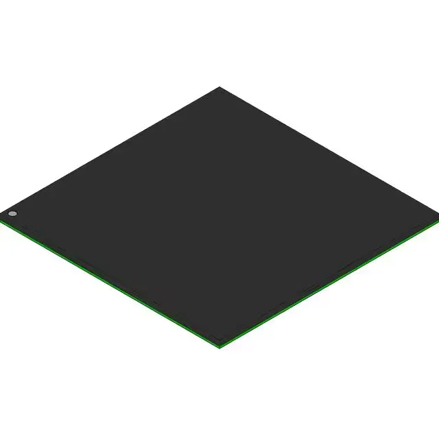
Lattice Semiconductor OR4E06-1BM680C — FPGA / CPLD & Programmable Logic
Technical Documents PDF / CAD
RoHS Compliant · Lead-Free EIA-481 Standard
Lattice Semiconductor / FPGA / CPLD & Programmable Logic

Lattice OR4E06-1BM680C FPGA, 899K gates, 466 I/O, ORCA4

MPN OR4E06-1BM680C
Active Spot Stock · 24-48h Dispatch 100% Original Sealed

Lattice Semiconductor ORCA4 FPGA, OR4E06-1BM680C, 899000 gates, 466 I/O, 151552 bits RAM, 1.425 V core, 0°C to 70°C, 680-pin BGA, Bulk.

Factory Allocation · Direct Sourcing
MOQ: 1 pcs
Logistics: DHL / FedEx DAP (Global Express · 3-7d) Russia & CIS DDP (Door-to-Door Cleared)
Dispatch: Shenzhen / HK
Wholesale Ref. Price (USD)
Target Price / Quote (2h Fast Turnaround)
Formal B2B Quotation in 2h
Volume pricing applies from 1,000 pcs upward, and is confirmed per order against the quantity and the shipment date. Inquire for Target Qty →
Working on a production BOM or have a target unit price? Submit Target Price
[SPEC] Essential Parameters Snapshot Full Specifications (11)
Supply Voltage 1.425

Full Technical Specifications

11 Parameters
OR4E06-1BM680C specifications
Parameter / AttributeSpecification / Value
SeriesORCA™4
MountingSurface Mount
Operating temperature high0°C to 70°C(TA)
Package_typeBulk
Number of i (O)466
Total ram bits151552
StatusActive
Number of gates899000
Supply voltage1.425
Number of labs (Clbs)2024
Number of logic elements (Cells)16192
[DESK] Shenzhen Spot Allocation · 2h Response

Need Immediate Spot Stock or Shortage Allocation for OR4E06-1BM680C?

Factory lead times blocking production? We lock verified brand-new original stock in Shenzhen within 2 hours.

Quote SLA 2 Hours
[01] Emergency Shortage 24-48h Shenzhen Dispatch

Direct access to Shenzhen floor inventory, franchised allocation buffers, and factory bonded stock to resolve line-down shutdowns.

[02] Industrial Packaging Tape & Reel / Tray / Tube

Standard factory-sealed packaging compliant with EIA-481 standards for automated high-speed SMT pick-and-place lines.

[03] WhatsApp QC Proof 45x Microscope QC Photos

High-resolution photos of original reel labels, 2D DataMatrix, and pin coplanarity sent via WhatsApp/Telegram before you release wire payment.

● USD Wire Transfer (SWIFT T/T) · DAP Express / DDP Delivery

Technical Details & Description

Logic density and I/O count for board-level integration

The OR4E06-1BM680C packs 899000 gates and 16192 logic elements in 2024 LABs — enough fabric to absorb a handful of 74-series glue-logic functions or a modest state machine without reaching for a larger die. 466 user I/O on a 680-ball BGA gives you the headroom to route a wide memory bus, a parallel LCD interface, and a dozen sensor interrupts without multiplexing — but the 1.425 V core rail means the I/O banks need their own supply sequencing if you are mixing 3.3 V peripherals. 151552 bits of on-chip block RAM (about 18.5 KB) is tight for a frame buffer but enough for a few small FIFOs or a coefficient lookup table — if your design needs more than a few hundred bytes of scratchpad, you will be budgeting an external SRAM or SPI flash.

Package and board-fit: 680-ball BGA

Surface-mount 680-ball BGA — the ball pitch and array dimensions are not in the spec table, but a package this dense typically requires a 4-layer PCB minimum for fan-out, with via-in-pad or microvias if the inner rows are used. Supplied in bulk (tray or tube, not tape-and-reel), so plan for manual or tray-fed pick-and-place — no reel changeover, but the handling is slower on a high-speed line.

Frequently asked questions

How does OR4E06-1BM680C compare to the Lattice XP2 series (LFXP2-17E-6FTN256C)?

The XP2 sibling (LFXP2-17E-6FTN256C) has 17000 logic elements and 282624 bits of RAM — about 5% more logic and nearly double the block RAM — but only 201 I/O in a 256-ball package. The OR4E06 gives you 466 I/O for wide-bus applications, while the XP2 offers more memory per logic cell. They are not pin-compatible; the BOM position determines the choice.

OR4E06-1BM680C
Verified Allocation
Quote