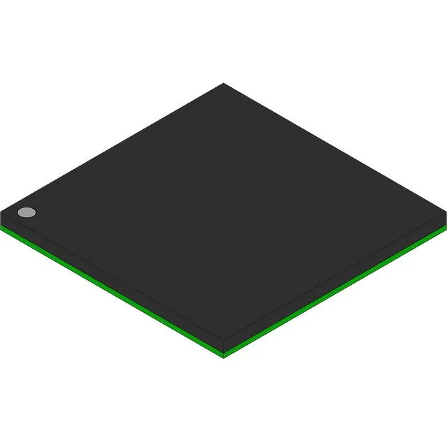
The OR2C15A4BA256-DB is a Lattice ORCA™2 FPGA with 44200 usable gates and 223 I/O pins. That I/O count is the headline number here — it lets you route a wide parallel bus (say a 16-bit data + address + control) alongside a bunch of discrete sensor or actuator lines without needing an external I/O expander or a second FPGA. On-chip RAM totals 25600 bits. That is enough for a small FIFO buffer, a register file for a soft-core state machine, or a few look-up tables — not enough for a frame buffer, but plenty for glue-logic scratchpad. The 1600 logic cells handle medium-density combinatorial and sequential logic — think address decoding, bus arbitration, or a simple custom peripheral interface. The commercial temperature range (0°C to 70°C) suits indoor equipment, lab instruments, and benchtop gear.
The supply voltage is 4.75 V — a legacy 5 V nominal rail.
Surface Mount package — the specific footprint is a 256-ball BGA. That means reflow assembly, not hand-soldering with an iron. A hot-air station or reflow oven is required; the pitch is fine enough that a stencil and paste are recommended for reliable joints. The 223 I/O fan out across the BGA grid. A 4-layer PCB with a dedicated ground and power plane is the practical minimum for signal integrity — two-layer boards will struggle to route the inner balls without vias stacking up.