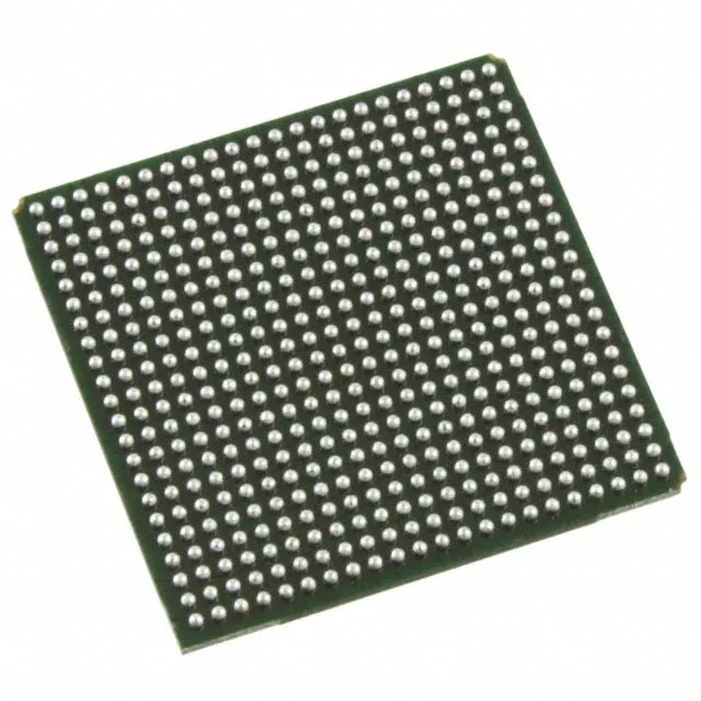
Active production — BOM-fit and logic density
The Lattice Semiconductor LFE3-70EA-7FN484C is an ECP3 family FPGA carrying 67000 logic elements and 4526080 total RAM bits, placing it in the mid- to high-density tier of the series for designs that need more fabric than the LFE3-35 but stay within the 484-ball FBGA footprint.
Memory budget and I/O planning
With 4.5 Mbit of block RAM distributed across 8375 logic slices, the memory-to-logic ratio supports moderate buffering and FIFO depth without resorting to external SRAM for many control-plane and packet-processing pipelines. 295 user I/O in a 484-ball FBGA means roughly 60% of the balls are signal pins — the rest are power and ground.
Sourcing posture — active, single-source line
For a procurement hedge, the LFE3-35EA-6FN484C shares the same 484-ball FBGA footprint and 295-I/O count but halves the logic fabric to 33000 LEs and cuts block RAM to 1.36 Mbit — a functional downgrade that requires re-timing the design, not a pin-compatible swap.