Logic capacity and I/O budget for mid-density designs
The LFE2-50E-5FN484I packs 48000 logic elements and 339 user I/O in a 484-ball FBGA — enough for a 32-bit RISC soft-core with a DDR memory controller and a dozen serial links without running out of routing channels. On-chip block RAM totals 396288 bits, which covers a 64 KB packet buffer or a moderate video line store; for larger memory, the 339 I/O leave room for an external DDR2/DDR3 bus.
Supply rail and temperature grade for industrial deployment
Core voltage is 1.14V — a single 1.2V rail with a 60 mV droop budget; the industrial junction range of -40°C to 100°C qualifies the part for outdoor base stations, factory-floor controllers, and engine-bay telematics without a commercial-grade derating. Compared to the sibling LFE2-50E-6FN484I, the -5 speed grade in this MPN trades a marginal timing margin for a wider operating envelope — the -6 grade offers a faster fmax but the same logic density and I/O count.
The ECP2 family is a mature mid-range node, so allocation risk is low compared to leading-edge FPGAs.
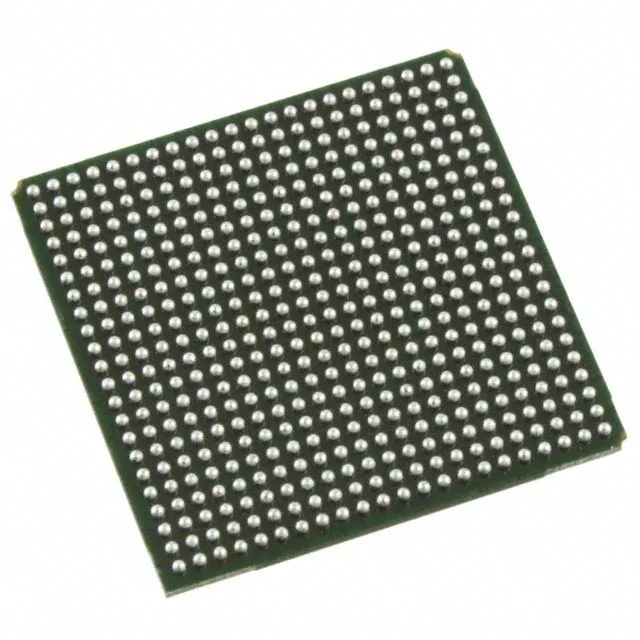
484-ball FBGA, 1.0 mm ball pitch — the fan-out needs a 4-layer PCB minimum; the centre thermal pad requires a 12×12 mm array of via-in-pad to keep junction temperature under 100°C at full toggle rate. The 339 I/O break out across eight banks with dedicated Vccio pins — each bank can run a separate voltage (1.8V, 2.5V, 3.3V) so mixed-voltage interfaces like LVDS and single-ended 3.3V live on the same die without level shifters.