Logic density and memory headroom for mid-density designs
The LFE5UM-85F-7BG381C packs 84000 logic elements and 21000 LABs/CLBs, placing it at the upper end of Lattice's ECP5 family for designs that need more fabric than the 44000-LE siblings but don't require the full gate count of a larger FPGA. On-chip block RAM totals 3833856 bits — roughly 3.8 Mbit — which buffers packet data, holds small look-up tables, or serves as line-rate FIFO memory without reaching for external SRAM.
I/O count and package — what fits on the board
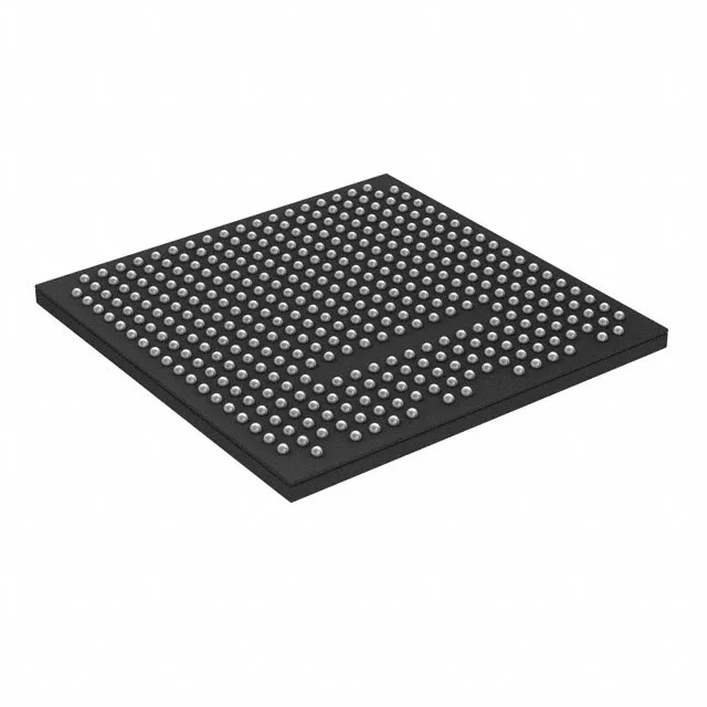
205 user I/O are brought out to a 381-ball CABGA (17x17 mm) — the 381-FBGA footprint is a common mid-density BGA that routes on a 4- to 6-layer PCB without exotic via-in-pad.
Temperature grade and deployment environment
It suits telecom line cards, test equipment, and industrial controllers that live in a conditioned or ventilated enclosure, but not extended outdoor or under-hood use. Production status is Active per Lattice's lifecycle record — no NRND or EOL notice on file.
How it compares to the LFE5UM-45F-8BG381C
Because both parts share the same 17x17 mm BGA footprint and supply voltage range, a board laid out for the 45F can accept the 85F as a drop-in upgrade — the extra I/O (205 vs 203) fits the same ball map, and the higher logic density is available without a PCB spin.