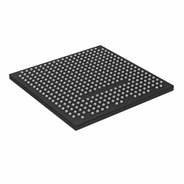
84K LUTs in a 17×17 mm CABGA — what the logic density means for your board
The LFE5U-85F-8BG381I is a Lattice ECP5 FPGA packing 84,000 logic elements (LUTs) and 21,000 LABs/CLBs into a 381-ball CABGA package measuring 17×17 mm. That logic density — roughly 290 LUTs per mm² of package footprint — makes it a fit for mid-complexity glue logic, sensor fusion, or video bridging where you need more fabric than the 45K or 25K ECP5 siblings but can't move to a larger BGA. On-chip block RAM totals 3,833,856 bits (just under 4 Mbit), distributed across the LAB array. For a design that fits in the 84K LUT budget, the memory is sized for typical line buffers or FIFO depths — not enough for a full frame store at 1080p, but sufficient for a few scan lines or a small packet buffer.
Package and reflow — what the 381-CABGA demands from the assembly line
The 205 user I/O fan out to the outer ball rows; inner rows carry core supply and ground. Core supply tolerance is tight: 1.045 V to 1.155 V. That means a 1.1 V rail with ±5 % regulation — a standard POL regulator or LDO with 1 % set-point accuracy covers it, but a 1.0 V rail with ±10 % tolerance won't hold the upper limit.
How it compares to the 45K and 25K ECP5 siblings
The closest peer in the same CABGA footprint is the LFE5UM-45F-7BG381I: 44,000 logic elements (roughly half the fabric), 1,990,656 bits of block RAM, and 203 I/O. The 85K part gives you 1.9× the LUT count and 1.9× the RAM in the same 381-ball layout — a board designed for the 45K can accept the 85K if the power supply can deliver the higher core current and the thermal budget handles the extra dissipation. The 256-ball siblings (LFE5U-45F-7BG256I and LFE5U-25F-8BG256I) share the same 17×17 mm body but with 197 I/O and a different ball map — they are not footprint-compatible with the 381-ball parts. A board laid out for the 256-ball package cannot accept the 85F-8BG381I without a layout spin.