Logic density and I/O budget for the BOM
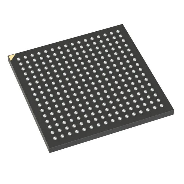
The LFE5U-25F-8BG256I: 24,000 logic elements (LUT4-based) in 6,000 LABs/CLBs — that is the fabric for a mid-complexity glue-logic or state-machine design, with enough headroom for a soft-core MCU plus peripheral decode without pinching the routing. 197 user I/O on a 256-ball CABGA — the ball pitch is 0.80 mm, so a 4-layer board with 5/5 mil trace/space can fan out the outer two rows; the inner rows need micro-vias or a via-in-pad if the board stack-up is tight.
On-chip memory and supply rails
1,032,192 bits (1 Mbit) of block RAM distributed as 36 Kbit EBR blocks — enough for a 256-byte FIFO per I/O bank or a moderate-size line buffer for a small display controller, but a full frame buffer for VGA at 24-bit colour would spill to external SDRAM. Core supply is 1.045 V to 1.155 V — a 1.1 V rail with ±5 % regulation covers it.
Temperature grade and environment
The part lives in an enclosure that sees ambient up to 85°C with a 15°C junction rise; above that the airflow or heatsink must keep Tj under 100°C or the timing model shifts. The 256-CABGA package is a 14x14 mm body, 1.0 mm max height, with a 0.80 mm ball pitch. The centre ground pad is not an exposed paddle — thermal relief goes through the solder balls to the PCB plane. A 2-second 260°C peak reflow profile per J-STD-020 works; moisture sensitivity level is MSL 3 (168-hour floor life) typical for this package family.
Speed grade and peer comparison
The -8 speed grade is the fastest standard option in the LFE5U-25 family — the sibling LFE5U-25F-6BG256I is a -6 grade, roughly 25 % slower on the worst-case timing paths (the exact delta depends on the design's critical path). If the board was laid out for the -6, the -8 drops in without any PCB change; the only difference is the speed bin, so the BOM line swaps directly. Stepping up to the LFE5U-45F-7BG256I doubles the logic to 44,000 cells and the block RAM to 2 Mbit, but the package stays 256-CABGA — same footprint, same ball-out. That is a real drop-in upgrade path if the design outgrows the 25K fabric, though the -7 speed grade is one notch below the -8.
The part ships in a tray, not tape-and-reel, so plan for pick-and-place with a tray feeder or a tube-to-tape conversion.