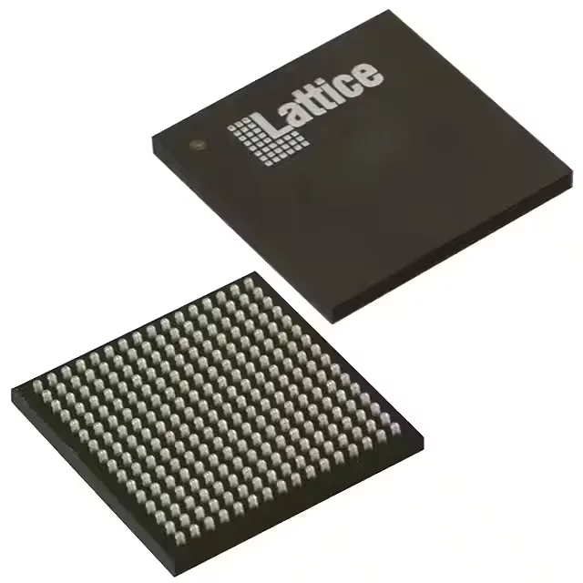
12000 logic cells, 197 I/O — the LFE5U-12F-7BG256I in the ECP5 family
The LFE5U-12F-7BG256I is a Lattice Semiconductor ECP5 FPGA with 12000 logic elements (3000 LABs/CLBs) and 197 user I/O, making it a mid-density device in the ECP5 family for cost-sensitive, low-power programmable logic applications. On-chip block RAM totals 589824 bits, enough for moderate FIFO, line buffer, or coefficient storage without external memory for many designs. The 256-CABGA (14x14 mm) package with 197 I/O demands a 4-layer or more PCB for fan-out of the 0.8 mm pitch BGA balls, typical for this density class.
Industrial temperature range and supply rails
Core supply is 1.045 V to 1.155 V — a tight 110 mV window that requires a regulated rail, not a raw board voltage. The 197 I/O banks can be configured with separate VCCIO rails, but the core rail must stay within this band for reliable operation. Surface-mount 256-LFBGA with a 14x14 mm body and 0.8 mm ball pitch — the same footprint as the 381-ball sibling, so a board laid out for the larger package can also accept this 256-ball variant if the extra I/O are not needed.