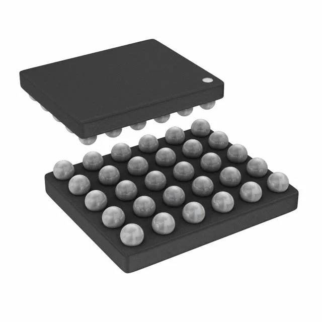
Lattice Semiconductor Corporation ICE40UP5K-UWG30ITR1K — FPGA / CPLD & Programmable Logic

Lattice ICE40UP5K-UWG30ITR1K FPGA, 5280 LEs, 21 I/O, WLCSP

MPNICE40UP5K-UWG30ITR1K
Active

Lattice Semiconductor Corporation iCE40 UltraPlus™ FPGA, ICE40UP5K-UWG30ITR1K, 5280 logic elements, 1.1 Mb SRAM, 21 I/O, 30-WLCSP (2.54x2.12 mm), -40°C to 100°C.

$8.8500Ref. price · indicative, final on quote
Packaging30-UFBGA, WLCSP
RoHSROHS3 Compliant
SeriesiCE40 UltraPlus™
Independent supplier — new & surplus stockAuthenticity-screened · ESD-safe packingListing updated Aug 2026

Specifications

ICE40UP5K-UWG30ITR1K specifications
ParameterValue
SeriesiCE40 UltraPlus™
MountingSurface Mount
Supply voltage1.14V ~ 1.26V
Operating temperature-40°C~100°C(TJ)
PackageTape & Reel (TR); Cut Tape (CT)
Number of i (O)21
Case30-UFBGA, WLCSP
Total RAM bits1171456
Number of LABs (CLBs)660
Number of logic elements (Cells)5280

Product details

5280 logic elements, 1.1 Mb SRAM — what the numbers mean for fit

The ICE40UP5K-UWG30ITR1K is an iCE40 UltraPlus FPGA with 5280 logic elements and 1,171,456 bits of block RAM. 21 user I/O in a 30-ball WLCSP (2.54 x 2.12 mm) means this part fits into a space where a larger BGA or QFN would not — think wearable or handheld edge devices where the PCB real estate is measured in millimeters. The 1.14 V to 1.26 V core supply is a single-rail affair; no separate VCCIO for the I/O banks, so the board-level decoupling is simpler than a multi-rail FPGA. A device sitting near a motor driver or a power supply in an enclosure that sees 85°C ambient still has 15°C of junction margin before the timing models shift.

ICE40UP5K vs ICE40UP3K — the real difference is memory

The closest sibling in the same WLCSP footprint is the ICE40UP3K-UWG30ITR1K. Both share the same 21 I/O, same 30-WLCSP package, same supply voltage range, and same temperature grade. The difference is inside: the UP5K packs 5280 logic elements and 1,171,456 bits of RAM, while the UP3K has 2800 logic elements and 1,130,496 bits of RAM. For a design that needs the extra logic cells — say a larger state machine or a soft-core processor — the UP5K is the right pick; if the logic fits in 2800 cells and the RAM budget is tight, the UP3K saves a few cents without a board respin.

Frequently asked questions

Where can I buy ICE40UP5K-UWG30ITR1K and get a price?

This part is sourced to order through independent distribution. Submit an RFQ for a firm price and lead-time commitment.

Will ICE40UP5K-UWG30ITR1K drop into a board designed for ICE40UP3K-UWG30ITR1K?

Yes — both parts share the same 30-WLCSP package, the same 21 I/O count, and the same supply voltage range. The footprint is identical, so a board laid out for the UP3K accepts the UP5K without any PCB change. The only difference is the logic density and RAM size.

What compliance documentation does Lattice provide for ICE40UP5K-UWG30ITR1K?

Lattice certifies this part as ROHS3 Compliant. The datasheet and PCN documentation are available from Lattice's website.