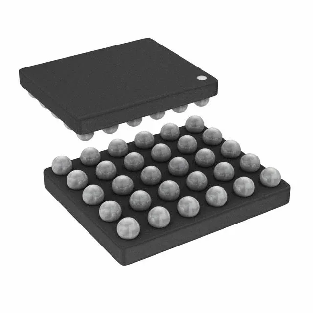
Logic density and on-chip memory in a 30-ball WLCSP
The ICE40UP3K-UWG30ITR1K packs 2800 logic cells (350 LABs) and 1 130 496 bits of SPRAM into a 30-ball WLCSP measuring 2.54 × 2.12 mm — the smallest footprint in the iCE40 UltraPlus family that still carries the full memory block. Twenty-one user I/O are available on the 30-ball array; the remaining balls are dedicated to power, ground, and configuration pins. The 1.14 V to 1.26 V core supply means the FPGA runs from a single 1.2 V rail — no separate VCCIO or VCCAUX needed for the logic fabric.
Industrial temperature range and package integration
A 2-layer PCB can route the 21 I/O if the fan-out is planned around the ball map; 4-layer boards give cleaner signal integrity for the SPRAM read/write paths.
Supplied in Tape & Reel (2500/reel) or Cut Tape, the WLCSP requires no special handling beyond standard MSL precautions for a 0.4 mm-pitch package. The laser-etched top marking should be consistent with Lattice's WLCSP marking convention — verify the date-code font against the factory's known laser etch pattern if the lot comes from a secondary source.