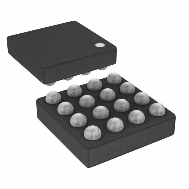
1248 logic cells in a 1.4x1.48 mm WLCSP — what that means for your BOM
The Lattice ICE40UL1K-SWG16ITR1K is an iCE40 UltraLite FPGA packing 1248 logic cells and 57 kbit of block RAM into a 16-ball WLCSP that measures just 1.4x1.48 mm. That cell count puts it in the smallest tier of the UltraLite family — enough for a few dozen LUTs of glue logic, a small state machine, or a serial bridge, but not for a soft-core processor or video pipeline. The 10 I/O count means this is a point-to-point part: a sensor interrupt, a chip-select, a UART or SPI link. Plan the pinout before layout because every ball is spoken for.
Package and rework reality — WLCSP on a 1.4x1.48 mm footprint
The 16-WLCSP has no exposed paddle and no corner pins to guide alignment — the only orientation mark is the ball pattern itself. Under a hot-air station, the part self-aligns on reflow if the solder paste is even, but lifting a mis-placed part risks lifting the pads because the die is nearly the same size as the package. A pre-bake at 125 °C for 8 hours is recommended if the reel has been opened longer than the MSL floor (the part is ROHS3, but MSL level is not stated in this record — treat it as MSL 1 or bake it). Place the decoupling caps within 2 mm of the WLCSP balls; a 100 nF 0201 X5R per supply ball is the starting point.
Active lifecycle — safe for new designs, but check the I/O count first
The industrial temperature range (-40 °C to 100 °C) covers outdoor enclosures, engine-bay auxiliary boards, and factory-floor sensor pods. The 1.14-1.26 V core is the only supply — no separate I/O bank voltage, so all 10 I/O swing at the core voltage level.