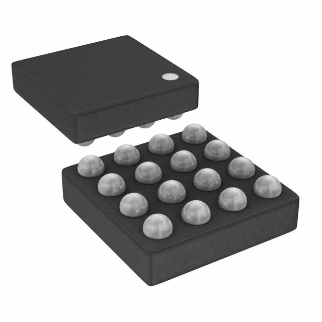
Active production — 640-LE iCE40 LP in a 1.4×1.48 mm WLCSP
The ICE40LP640-SWG16TR1K is an active-production Lattice iCE40 LP FPGA with 640 logic elements across 80 LABs, 32 Kbit of block RAM, and 10 user I/O — all in a 16-ball WLCSP that measures 1.4×1.48 mm.
Package and supply — what the WLCSP-16 means for the board
The 16-XFBGA, WLCSP package (supplier device package 16-WLCSP, 1.4×1.48 mm) is a wafer-level chip-scale package with no mould compound — the die backside is the package top. This gives the smallest footprint in the iCE40 LP family but requires a PCB with fine-line traces (0.2 mm / 0.2 mm design rules typical) and a controlled-collapse solder-joint profile. The 10 I/O are distributed across the ball grid; the remaining balls are power and ground. The 1.14 V to 1.26 V supply must be within 60 mV of the nominal 1.2 V — a standard 1.2 V LDO with 1% accuracy covers it.
Logic density and memory — sizing the part against the task
640 logic elements (80 LABs of 8 LEs each) and 32 Kbit of block RAM position the ICE40LP640 as a glue-logic or small-state-machine FPGA. The 32 Kbit RAM is organised as 4 Kbit blocks — enough for a small FIFO, a coefficient lookup table, or a line buffer for a low-resolution display. The 10 I/O limit the external interface width; typical applications are SPI/I2C bridge, sensor aggregation, or a simple PWM generator. For designs needing more RAM or logic, the ICE40UL1K-SWG16ITR1K (same package, 1248 LEs, 57344 bits RAM) is a pin-compatible step up.