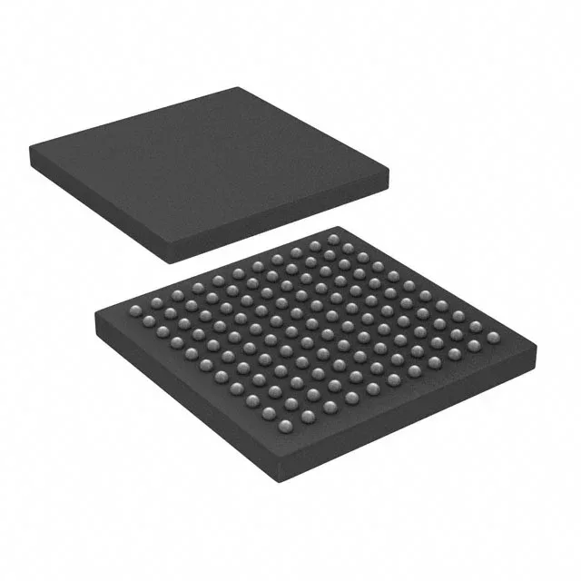
Lattice Semiconductor Corporation ICE40HX8K-BG121 — FPGA / CPLD & Programmable Logic
Technical Documents PDF / CAD
RoHS Compliant · Lead-Free EIA-481 Standard
Lattice Semiconductor Corporation / FPGA / CPLD & Programmable Logic

Lattice ICE40HX8K-BG121 FPGA, 7680 LEs, 93 I/O, 121-caBGA

MPN ICE40HX8K-BG121
Active Spot Stock · 24-48h Dispatch 100% Original Sealed

Lattice Semiconductor Corporation iCE40™ HX FPGA, ICE40HX8K-BG121, 7680 logic elements, 93 I/O, 128 Kbit RAM, 121-caBGA (9x9), -40°C to 100°C, Tray.

In Stock: 1,240 pcs
MOQ: 1 pcs
Logistics: DHL / FedEx DAP (Global Express · 3-7d) Russia & CIS DDP (Door-to-Door Cleared)
Dispatch: Shenzhen / HK
Unit Price (USD)
$14.25 / pc
Direct Purchase Ready
Volume Pricing Breaks Confirmed upon quotation
1+ pcs
$14.25
10+ pcs
$12.83
30+ pcs
$11.69
100+ pcs
$10.55
500+ pcs
$9.83
1,000+ pcs
$9.26
Working on a production BOM or have a target unit price? Submit Target Price
Buy Now

$14.25 / ea

1,240 in stock — maximum per order · 3–4 days lead time

$12.83 / ea from 10 pcs

Upload Full BOM List
[SPEC] Essential Parameters Snapshot Full Specifications (10)
Package / Case 121-TFBGA
Supply Voltage 1.14V ~ 1.26V
ALT
Facing long factory lead times or allocation on ICE40HX8K-BG121? Verified pin-compatible alternatives available with active Shenzhen stock and 100% solder-ready footprint match.

Full Technical Specifications

10 Parameters
ICE40HX8K-BG121 specifications
Parameter / AttributeSpecification / Value
SeriesiCE40™ HX
MountingSurface Mount
Supply voltage1.14V ~ 1.26V
Operating temperature-40°C ~ 100°C (TJ)
PackageTray
Number of i (O)93
Case121-TFBGA
Total RAM bits131072
Number of LABs (CLBs)960
Number of logic elements (Cells)7680
100% Footprint Match · Solder-Ready (No PCB Redesign Needed)

Need Stock or a Drop-in Second-Source for ICE40HX8K-BG121?

Package: QFN / ucBGA / WLCSP / TQFP · Pin-compatible replacements with immediate Shenzhen spot stock

Footprint Match 97%
Supply Chain & Allocation Reality:

The iCE40 line is the FPGA family that the hobby and small-batch world actually uses - and the data says the same thing about buyers: searches concentrate on Lattice CPLD and iCE40 class parts while Xilinx orderables sit at the noise floor. The family is five sub-splits with wildly different capabilities (UltraLite to UltraPlus) sharing a naming theme and a common trait: an SRAM fabric that must be loaded at every power-up - from an external SPI flash, a host CPU, or the family-internal NVCM. The sourcing consequence is structural: an iCE40 socket is never just an FPGA line on the BOM; it is a two-part relationship with a configuration memory.

Verified Pin-Compatible Replacements (3 verified alternatives)

iCE40UP5K Lattice Semiconductor QFN-48 / SG48 / WLCSP
Functional Equivalent
Availability & Target Pricing:

The UltraPlus Flagship

Shenzhen Spot Stock (24-48h Dispatch)

Electrical & Core Specs:

The richest sub-split: 5,280 LUTs with 1Mb of SPRAM (four 256kb blocks), DSP blocks, two hardened SPI and two I2C blocks, and on-chip oscillators - built for always-on sensor buffering and audio pre-processing.

Low-power single-rail design point; the UltraPlus is the part behind most current iCE40 designs.

Compatibility & Drop-In Notes: Sub-splits are not interchangeable: LP/HX/Ultra/UltraLite/UltraPlus differ in logic, memory and hardened IP. Replacing one with another is a re-synthesis and placement project, and the pin maps differ even in the same package size.
Package & Solder Footprint: Common QFN-48-class outlines are shared - verify pin map against the exact device, not the package.
Shenzhen Warehouse Stock & MOQ: Stocked with config flash paired on request (W25Q-class SPI flash sourced on the same order).
iCE40HX1K Lattice Semiconductor TQFP-144 / VQFP-100 / QFN
Functional Equivalent
Availability & Target Pricing:

The Performance Sub-Split

Shenzhen Spot Stock (24-48h Dispatch)

Electrical & Core Specs:

The HX line trades standby current for more logic per die (HX1K/4K/8K against LP1K/4K/8K); the classic hobby board part of the iCE40 generation.

Low-power but not the micropower LP class; check the static current against the design budget.

Compatibility & Drop-In Notes: LP and HX are the two faces of the same generation: the pin maps match within a device size, but the power and clocking characteristics differ. In repair of hobby-era boards, match the exact device.
Package & Solder Footprint: Larger through-hole-friendly VQFP/TQFP outlines exist in this line.
Shenzhen Warehouse Stock & MOQ: Stocked for repair of the hobby and education ecosystem boards.
ECP5 Lattice Semiconductor caBGA / csBGA families
Functional Equivalent
Availability & Target Pricing:

The Step-Up Platform

Shenzhen Spot Stock (24-48h Dispatch)

Electrical & Core Specs:

The next class above iCE40 in the Lattice stack: higher logic density and hardened high-speed interfaces for video, networking and instrumentation designs.

Multi-rail FPGA supply design - not a drop-in to any iCE40 socket.

Compatibility & Drop-In Notes: Listed to complete the Lattice map - the two families share tooling (Lattice Radiant) but nothing electrical. The honest cross-family statement: re-design, not replacement.
Package & Solder Footprint: BGA-only packaging; assembly and inspection requirements differ from iCE40 QFN work.
Shenzhen Warehouse Stock & MOQ: Stocked per part number with photographed markings - BGA FPGAs are a favored relabeling target.
Buyer & Quality Checklist for Sourcing Alternatives
  • Every iCE40 is SRAM-based: the design lives in configuration memory loaded at power-up (external SPI flash, host controller, or NVCM where present). A board without its config flash is a board with a blank FPGA - when sourcing iCE40, source the paired W25Q-class flash on the same order.
  • The five sub-splits (UltraLite / LP / HX / Ultra / UltraPlus) are different devices, not grades of one device: logic, memory, DSP and hardened IP differ, and the same-size package does not imply the same pin map.
  • Small packages drop features: several mini outlines have no PLL, and the constant-current LED sink exists on selected packages only. The package letter in the orderable number is a spec, not a shipping choice.
  • NVCM configurations are instant-on and secure but one-shot - production planning for NVCM-programmed devices needs lead time and programming decisions upstream, not at the bench.
  • The market leans Lattice for this class (buyer searches concentrate here, not on Xilinx orderables): keep depth in iCE40 and the config flash, with ECP5 quoted case-by-case.
  • iCE40 boards in the repair channel are numerous (hobby, education, instrumentation): the two failure parts are the FPGA and its config flash - check the flash first, it is cheaper and it holds the bitstream.
Frequently Asked Technical Questions

Q: Which iCE40 sub-family do I need?

A: Choose by need: UltraPlus (UP5K) when on-chip SPRAM or DSP is required; HX/LP for general low-power logic with more density; Ultra for mobile glue logic with hardened SPI/I2C; UltraLite for the absolute smallest always-on designs. Sub-splits are not interchangeable.

Q: Does iCE40 need an external flash chip?

A: It configures at every power-up: from an external SPI flash in self-boot mode, from a host CPU in slave mode, or from the internal NVCM where the design was programmed there. Most boards carry a small W25Q-class SPI flash for the bitstream - source it with the FPGA.

Q: Can I replace a dead iCE40 with an ECP5?

A: No - different family, different packaging and supply design. ECP5 is the step-up platform for higher density and interfaces; migrating is a re-layout and re-synthesis project.

Technical Details & Description

7680 logic elements in a 9x9 mm BGA

The ICE40HX8K-BG121 is a Lattice iCE40 HX family FPGA packing 7680 logic elements and 128 Kbit of block RAM into a 121-ball caBGA package that measures 9x9 mm. That logic density in a hand-assembly-friendly BGA footprint makes it a candidate for glue-logic consolidation or sensor-bridge processing where board real estate is tight. Ninety-three general-purpose I/O are available, which for a 121-ball package means a high I/O-to-ball ratio — most of the balls are signal, not power or ground. That suits designs where you need to interface to a parallel bus or a bank of sensors without giving up half the package to supply rails. The 1.14 V to 1.26 V core supply means a single 1.2 V rail powers the fabric; no separate VCCIO for the core.

Package and board-fit considerations

The 121-caBGA (9x9 mm) has a 0.8 mm ball pitch — a standard 4-layer PCB with via-in-pad can route all 93 I/O. The 0.8 mm pitch is forgiving enough for most rework stations; a hot-air rework profile with bottom-side preheat handles removal without lifting pads. Supplied in Tray packaging, not tape-and-reel.

Frequently asked questions

Is the ICE40HX8K-BG121 pin-compatible with the ICE40HX8K-CT256?

No. The ICE40HX8K-CT256 uses a 256-ball CTBGA package with 206 I/O, while the BG121 uses a 121-ball caBGA with 93 I/O. The ball maps are different; a board designed for the CT256 will not accept the BG121 without a layout change.

What is the difference between the ICE40HX8K-BG121 and the ICE40LP8K-CM121?

Both share the same logic density (7680 LEs, 128 Kbit RAM) and the same 121-ball BGA footprint. The HX variant is the high-performance member of the iCE40 family, while the LP variant is the low-power member. The HX typically has a faster maximum frequency at the cost of higher dynamic power. The pinout is identical, so a board can accept either depending on the power/performance target.

ICE40HX8K-BG121
Verified Allocation
Quote