15 ns propagation delay — what it means for logic timing
The GAL16V8ZD-15QJ: The 15 ns pin-to-pin propagation delay sets the ceiling for combinatorial logic paths through the device. Any signal that must ripple through multiple PAL blocks in sequence accumulates this delay per stage — a three-level decode path budgets 45 ns minimum before the output settles. For registered outputs, the 15 ns figure also governs the maximum clock-to-output time. The internal feedback path from the macrocell register back into the logic array adds another 5–7 ns, so the effective system clock rate tops out around 40–50 MHz in practice.
8 macrocells — glue-logic consolidation target
Eight macrocells, each configurable as registered or combinatorial output with programmable polarity, replace roughly 8–12 discrete 74-series logic packages on a board. The EE PLD cell retains the configuration when power is removed — no external boot PROM needed. The 4.75V to 5.25V supply rail matches legacy 5V TTL systems. If the rest of the board has migrated to 3.3V, a level translator on the I/O lines is required — the GAL16V8ZD-15QJ does not tolerate a 3.3V-only supply.
20-PLCC footprint and rework considerations
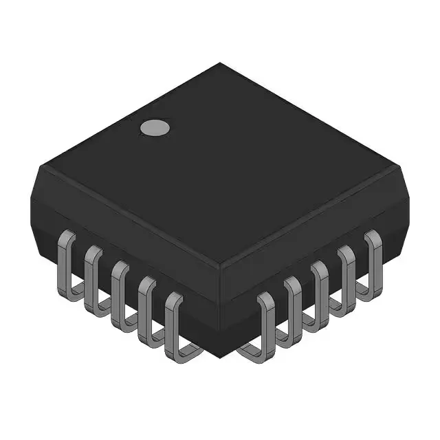
The 20-PLCC (J-Lead) package measures 9x9 mm with a 1.27 mm pitch. The J-lead profile sits below the package body, so inspection requires a side-view scope or X-ray — the solder joints are hidden under the package overhang. Rework with hot air is straightforward: preheat the board to 100–120°C, then focus the nozzle on the package body until the solder under all four sides reflows. The J-lead footprint is less prone to tombstoning than gull-wing, but the pad geometry must match the PLCC land pattern — a SOIC footprint will not align.
Active lifecycle — no end-of-line pressure
RoHS non-compliant — the lead finish on the J-leads contains lead. This is typical for legacy PLCC parts and is exempt under RoHS Annex III for high-reliability and industrial applications. Confirm your assembly house's exemption policy before committing the BOM.