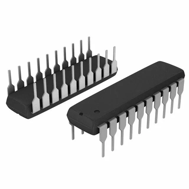
The GAL16V8D-25QPI is officially obsolete per Lattice Semiconductor's lifecycle status.
8 macrocells — the logic capacity anchor
Eight macrocells define the usable logic density — each macrocell contains a programmable AND array feeding a configurable OR term, plus a flip-flop that can be bypassed for combinatorial output. This is the same architecture as the original GAL16V8, so existing JEDEC fuse maps from that family load directly. The 25 ns propagation delay (25QPI speed grade) sets the maximum system clock rate — at 25 ns, the part supports toggle rates up to roughly 40 MHz in registered mode, though the actual ceiling depends on the external feedback path and output loading.
20-DIP through-hole — legacy socket compatibility
The 20-pin DIP (0.300-inch row spacing) is the standard GAL16V8 footprint. The through-hole package simplifies hand-prototyping and field replacement but limits board density compared to surface-mount alternatives. The EE PLD programmable type means the device is electrically erasable — it can be reprogrammed in a standard PLD programmer without UV erasure. No windowed package is used, so the part is OTP in the sense that it cannot be erased optically, but the EE cell supports multiple program/erase cycles.