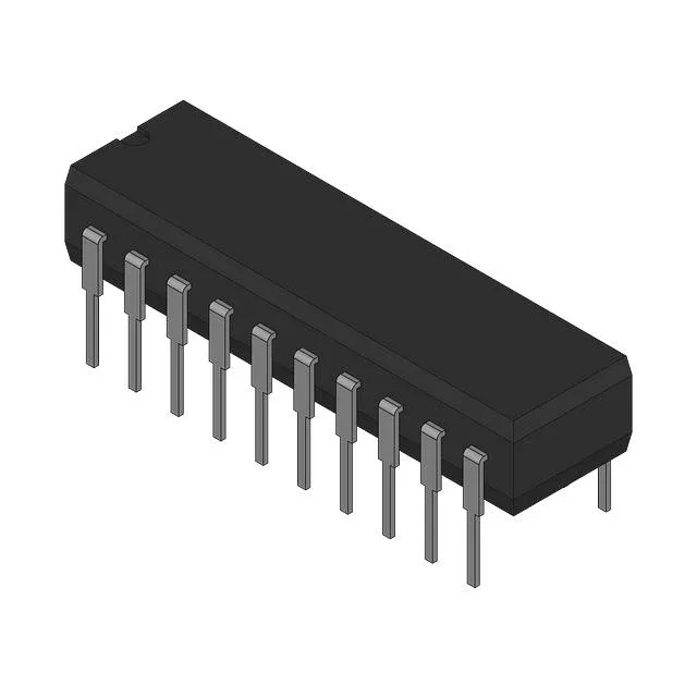
Lattice Semiconductor Corporation GAL16V8C-5LP — FPGA / CPLD & Programmable Logic

Lattice GAL16V8C-5LP CPLD, 5 ns, 8 macrocells, 20-DIP

MPNGAL16V8C-5LP
Active

Lattice Semiconductor Corporation GAL® 16V8 series EE PLD, GAL16V8C-5LP, 5 ns speed, 8 macrocells, 4.75V–5.25V supply, 20-DIP (0.300", 7.62mm) through-hole package, bulk.

$5.6100Ref. price · indicative, final on quote
Packaging20-DIP (0.300", 7.62mm)
RoHSRoHS non-compliant
SeriesGAL® 16V8
Independent supplier — new & surplus stockAuthenticity-screened · ESD-safe packingListing updated Aug 2026

Specifications

GAL16V8C-5LP specifications
ParameterValue
SeriesGAL® 16V8
MountingThrough Hole
Programmable typeEE PLD
Voltage - input4.75V ~ 5.25V
Speed5 ns
PackageBulk
Case20-DIP (0.300\", 7.62mm)
Number of macrocells8

Product details

5 ns pin-to-pin — timing budget for address decode and glue logic

The GAL16V8C-5LP is a 5 ns EE PLD from Lattice's GAL® 16V8 series, offering 8 macrocells in a 20-pin DIP package. The 5 ns propagation delay sets the timing margin for combinatorial decode paths — a 50 MHz address bus needs the output valid before the next clock edge, and this part delivers that headroom without adding wait states. It operates from a 4.75V to 5.25V supply rail, placing it in the legacy 5V-only logic family. The through-hole 20-DIP (0.300", 7.62mm) body is socketable or wave-solderable, and the 20-PDIP footprint matches the industry-standard GAL16V8 pinout — a drop-in replacement for earlier 20-pin PAL/GAL devices in existing boards.

The 5 ns speed grade is the fastest in the GAL16V8C family; if the timing budget allows a 7.5 ns window, the GAL16V8C-7LP (same pinout, same 8 macrocells) is a direct parametric alternative that may offer better supply depth.

Frequently asked questions

What is the GAL16V8C-5LP's speed and how does it affect timing?

The listed speed is 5 ns pin-to-pin propagation delay (combinatorial path). This sets the maximum clock frequency for registered outputs and the address-to-output valid window for decode logic — a 5 ns delay means the output settles within one 200 MHz clock period, though the practical system clock is limited by the external routing and load capacitance.

Will the GAL16V8C-5LP drop into a board originally built with the GAL16V8C-7LP?

Yes — both parts share the same 20-pin DIP footprint, 5V supply range, 8 macrocells, and JEDEC fuse-map architecture. The only difference is the speed grade: 5 ns vs 7.5 ns. The 5 ns part is a superset — it meets or exceeds the 7.5 ns timing, so no board rework is needed.

What compliance documentation is available for the GAL16V8C-5LP?

Lattice provides the datasheet and programming specification for the GAL16V8C family. The part is RoHS non-compliant (tin-lead finish).