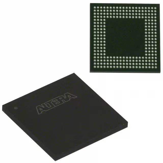
440 macrocells, 5.4 ns pin-to-pin — the logic-density decision
The Intel EPM570M256I5N is a MAX II CPLD packing 440 macrocells and 570 logic elements in a 256-ball MBGA (11x11 mm) footprint. That 5.4 ns max propagation delay (tpd1) sets the combinatorial path ceiling — glue logic that must resolve within one clock edge at 100+ MHz needs this speed grade, not the slower 7 ns variant in the same family. With 160 user I/O distributed across the 256-TFBGA, the part fits medium-density bus interfaces and memory controllers where a smaller 80-I/O MAX II (EPM240) would force a board spin.
Dual-supply routing and in-system programming
The core runs on 2.5 V while the I/O banks accept 3.3 V — a common split for bridging a 2.5 V FPGA core to 3.3 V peripherals without external level shifters. The supply rails must be sequenced per Intel's MAX II power-up guidelines; the device is in-system programmable via the JTAG interface, so firmware updates happen on the assembled board through the standard 10-pin header. The 256-MBGA (11x11 mm) uses a 0.80 mm ball pitch — a 4-layer PCB with via-in-pad or dogbone fan-out handles the breakout without microvias. The exposed center pad (if present on this variant) should be stitched to the ground plane with at least 9 thermal vias to keep the junction temperature below the 100°C ceiling under continuous operation.
Active lifecycle — no last-time-buy pressure
The MAX II family is mature but still supported; Intel's Quartus Prime software (free edition) targets this device without a license key. For a BOM that already qualified the 256-MBGA footprint, the closest sibling is the MAX V 5M570ZF256I5N — same 440 macrocells and 570 LEs, same -40°C to 100°C range, but with a 1.8 V core instead of 2.5 V/3.3 V and a 9 ns tpd (slower). The pinout is not identical; a board respin is required to migrate between the two families.