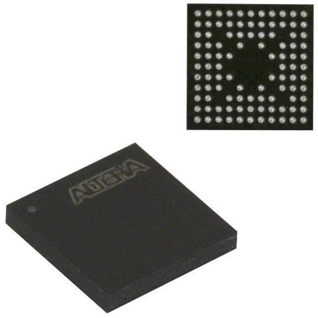
Intel EPM570GM100I5N — FPGA / CPLD & Programmable Logic

Intel EPM570GM100I5N MAX II CPLD, 440 Macrocells, 5.4 ns

MPNEPM570GM100I5N
Active

Intel MAX® II CPLD, EPM570GM100I5N, 570 logic elements, 440 macrocells, 76 I/O, 5.4 ns pin-to-pin delay, 1.71V–1.89V core, 100-TFBGA, -40°C to 100°C.

$300.0000Ref. price · indicative, final on quote
Independent supplier — new & surplus stockAuthenticity-screened · ESD-safe packingListing updated Aug 2026

Specifications

EPM570GM100I5N specifications
ParameterValue
SeriesMAX® II
MountingSurface Mount
Programmable typeIn System Programmable
Voltage supply - internal1.71V ~ 1.89V
Operating temperature-40°C~100°C(TJ)
PackageTray
Number of i (O)76
Case100-TFBGA
Number of macrocells440
Delay time tpd(1) max5.4 ns
Number of logic elements (Blocks)570

Product details

The Intel EPM570GM100I5N is a MAX® II family CPLD with 570 logic elements and 440 macrocells in a 100-ball TFBGA (6x6 mm MBGA) package. It delivers a 5.4 ns pin-to-pin propagation delay and provides 76 user I/O, making it a fit for board-level glue logic, address decoding, bus bridging, and power-up sequencing in industrial control, telecom, and motor-drive applications.

The 100-TFBGA package keeps the footprint small (6x6 mm), but the BGA requires controlled soldering profiles and X-ray inspection — factor that into assembly cost if your line is used to QFP packages.

Frequently asked questions

What are the equivalent parts for EPM570GM100I5N?

No direct pin-compatible second source exists within the MAX II family. The older MAX 7000 series parts (EPM7128BFC256-7, EPM7128ALC84-6, EPM7128ATI144-10) are different voltage, density, and package families — not functional equivalents.

Is EPM570GM100I5N compatible with 3.3V logic?

The core supply is 1.71 V to 1.89 V, but the I/O banks can interface with 3.3 V logic if the VCCIO pins are supplied at 3.3 V. Check the MAX II datasheet for VCCIO configuration details.

What is the pinout of EPM570GM100I5N?

The pinout is defined in the MAX II device family datasheet for the 100-TFBGA package. The 76 I/O are arranged in four banks with dedicated VCCIO and GND balls. Refer to the official Intel/Altera pinout table for ball assignments.