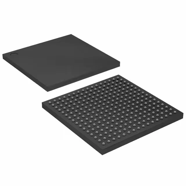
440 macrocells at 5.4 ns – the glue-logic workhorse
The EPM570F256I5 is an Intel MAX II CPLD packing 440 macrocells and 570 logic elements in a 256-ball FBGA (17x17 mm). With a propagation delay (tpd) of 5.4 ns max, it handles address decoding, bus bridging, and I/O expansion at speeds that keep up with a 100+ MHz system clock without adding wait states.
Active production – no last-time-buy scramble
The commercial-grade sibling (EPM570F256C5, 0°C to 85°C) is the cost-down option if your environment stays indoors.
In-system programmable – no socket, no UV eraser
The MAX II family is in-system programmable via a standard JTAG interface (IEEE 1149.1). You can program it on the board after soldering – no separate programmer socket or UV eraser needed. The non-volatile configuration is stored in flash cells, so the part boots immediately on power-up without an external configuration memory. Programming is done through Intel Quartus Prime software (standard or Lite edition) using the JTAG chain. The same tool handles design entry, synthesis, place-and-route, and timing analysis for the 5.4 ns tpd target – no separate simulator license required for a CPLD of this density.
256-FBGA footprint – layout reality check
The 256-ball FBGA measures 17x17 mm with a 1.0 mm ball pitch. That pitch is forgiving enough for a 4-layer PCB with via-in-pad if your layout is tight, but a 6-layer board gives cleaner breakout for the 160 I/O plus the VCCINT (2.5 V) and VCCIO (3.3 V) supply planes. The centre of the package has no thermal pad – the die dissipates through the BGA balls and the PCB copper – so ensure adequate via stitching under the package to the ground plane.