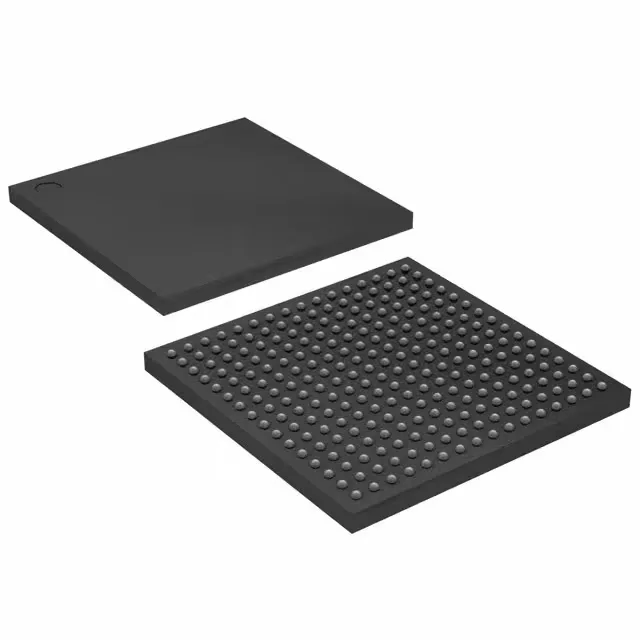
980 macrocells in a 17×17 mm BGA — the glue-logic workhorse
The Intel EPM1270F256C5 is a MAX® II CPLD packing 980 macrocells and 1270 logic elements into a 256-ball FBGA footprint measuring 17×17 mm. The 212 user I/O break out from the 256-ball array, leaving 44 balls for power and ground — a ratio that keeps simultaneous switching noise manageable if the board layout follows the recommended decoupling scheme. The dual-voltage supply (2.5 V core, 3.3 V I/O) matches common 3.3 V peripheral rails while keeping the core power low.
6.2 ns tpd — what that means for timing closure
The 6.2 ns tpd(1) max is the pin-to-pin delay through a single LUT — the fastest path the datasheet guarantees. For a 50 MHz bus interface, the period is 20 ns; after subtracting setup/hold and clock skew, the combinatorial logic budget is roughly 10–12 ns, so a single level of logic fits comfortably. Two levels in series (12.4 ns) start eating into the margin and may require pipelining or a faster speed grade. In-system programmability via JTAG means the part can be programmed on the board after assembly — no socket, no pre-programmed inventory. The MAX II family uses a flash-based configuration cell that retains the design at power-off, so there is no external configuration memory needed.
256-FBGA — board-fit and hand-solderability
No extended or automotive temperature rating, so it is not suited for under-hood or outdoor enclosures without active cooling.
Active lifecycle — no end-of-life pressure
The base product number is EPM1270; the F256C5 suffix denotes the 256-FBGA package and the C5 speed grade (the fastest commercial-grade option in this density). The same die is available in a 144-pin TQFP (EPM1270T144C5) if the BGA is a layout concern, though the I/O count drops to 116.