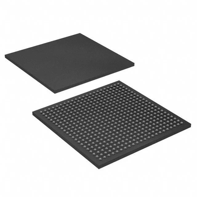
Intel 10M50DDF484I7G — FPGA / CPLD & Programmable Logic

Intel 10M50DDF484I7G MAX 10 FPGA, 50K LEs, 360 I/O, 484-BGA

MPN10M50DDF484I7G
Active

Intel MAX® 10 FPGA, 10M50DDF484I7G, 50000 logic elements, 360 I/O, 1677312 total RAM bits, 2.85V–3.465V supply, -40°C to 100°C industrial, 484-FBGA (23x23), Tray.

$286.6300Ref. price · indicative, final on quote
StockContact for availability
MOQ1 pcs
  • 100% new & originalTraceable channels only — no refurbs, no pulls, no remarked parts.
  • Date & lot codes on quoteStated per line before you commit; label photos on request.
  • MSL-compliant ESD packingMoisture-sealed bags with indicator cards; reels photo-verified.
  • PayPal buyer protectionPay by T/T, PayPal or Payoneer — card payments covered end to end.

Specifications

10M50DDF484I7G Technical Specifications
ParameterValue
SeriesMAX® 10
Mounting typeSurface Mount
Voltage2.85V ~ 3.15V, 3.135V ~ 3.465V
Operating temperature-40°C ~ 100°C (TJ)
PackageTray
Number of i (O)360
Case484-BGA
Total RAM bits1677312
Number of LABs (CLBs)3125
Number of logic elements (Cells)50000

Product details

MAX 10 at 50K LEs — where this density lands

The Intel 10M50DDF484I7G is a MAX® 10 FPGA with 50000 logic elements, 360 user I/O, and 1677312 bits of embedded RAM in a 484-ball FBGA package.

Industrial temperature — what it buys you

Rated -40°C to 100°C junction temperature. The 100°C TJ limit is the hard ceiling.

Active lifecycle — no allocation pressure yet

Intel lists the 10M50DDF484I7G as Active. No NRND flag, no last-time-buy notice on the MAX 10 family at this density. That means the part is still in normal production through franchised distribution. The spot market sees occasional excess from over-ordered builds, but the primary channel is the cleanest route. If you are stocking for a five-year production run, this is not a part that needs a lifetime buy today — just keep an eye on Intel's quarterly PCNs for any package or wafer-fab changes.

Programming and configuration

MAX 10 devices embed non-volatile flash configuration memory — no external configuration PROM needed. The 10M50DDF484I7G powers up and loads its image from internal flash, which simplifies the board layout and reduces BOM count. Programming is done through the JTAG interface using Intel Quartus Prime; the same interface handles in-system debugging via Signal Tap. For production programming, a dedicated flash programmer or a boundary-scan chain handles multiple devices on the same board.

Frequently asked questions

What is the closest functional second-source to 10M50DDF484I7G?

The 10M40DCF484I7G is the nearest density step down within the same MAX 10 family — same 360 I/O, same 484-FBGA package, same industrial temperature range, but with 40000 logic elements instead of 50000. It is a pin-compatible drop-in for designs that fit in the smaller density.

What is the datasheet for 10M50DDF484I7G?

The Intel MAX 10 FPGA device datasheet covers the full family including the 10M50DDF484I7G. It documents the logic array, embedded memory blocks, PLLs, I/O standards, and configuration details.

What are the programming options for 10M50DDF484I7G?

The MAX 10 family uses internal flash configuration memory, so no external configuration device is needed. Programming is done through the JTAG interface using Intel Quartus Prime software.