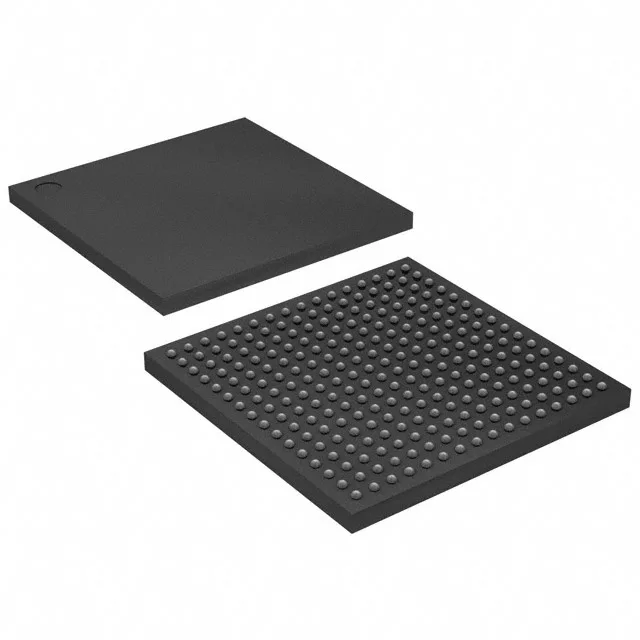
50K logic elements, 178 I/O, 256-FBGA — what this MAX 10 FPGA carries
The Intel 10M50DCF256C7G is a MAX® 10 FPGA with 50000 logic elements and 178 user I/O, packed in a 256-FBGA (17x17 mm) surface-mount package. It carries 1677312 bits of on-chip RAM, enough to buffer a full VGA frame or hold a moderate packet queue without external memory.
Active lifecycle — no last-time-buy pressure
Intel lists the 10M50DCF256C7G as Active. The MAX 10 family has broad distribution, so sourcing through independent channels is straightforward.
Package and board-fit — 256-FBGA, 17x17 mm
The 256-FBGA (17x17 mm) package uses a 1.0 mm ball pitch — it routes out on a standard 4-layer PCB without microvias. The 178 I/O are distributed across the ball array; the centre balls are core power and ground, so the board layout needs a solid via-in-pad or dog-bone fan-out for the supply rails. Supplied in tray format, not tape-and-reel — this is typical for BGA devices that go through pick-and-place with a tray feeder.
On-chip RAM and logic density — what 1.6 Mbit and 3125 LABs mean
The 1677312 total RAM bits are organized as M9K blocks — each block is 9 Kbit, so this part carries roughly 186 blocks. That is enough for a 64-byte-wide FIFO that is 256 entries deep, or a small coefficient table for a digital filter. The 3125 LABs/CLBs each contain 16 logic elements, giving fine-grained control over combinatorial and registered logic. Compared to the 10M40DCF256C8G, which has 40000 logic elements and 1290240 RAM bits, this 10M50 part offers 25% more logic and 30% more RAM in the same 256-FBGA footprint. If your design is already on the 10M40 and the fit is tight, the 10M50 is a drop-in upgrade — same package, same I/O count, same supply rails.