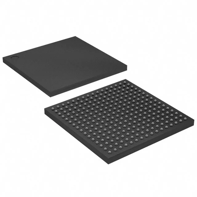
40K LE FPGA with 500 I/O in a 672-ball BGA
The 10M40DDF672I7G: This is the high-I/O-density variant of the 40K LE family — the 500 I/O count gives you enough pins to interface with wide memory buses, multiple parallel ADCs, or a bank of sensors without resorting to external muxing. On-chip memory totals 1290240 bits (roughly 1.25 Mbit), which is enough for a small frame buffer, coefficient tables, or a FIFO for data aggregation before the external memory controller kicks in. The dual supply voltage range — 2.85V to 3.15V for the core and 3.135V to 3.465V for the I/O banks — means you can run the logic from a 3.0V rail while keeping the I/O at standard 3.3V levels without a separate regulator.
Industrial temperature grade and package fit
The 672-FBGA package demands a multi-layer PCB with via-in-pad or microvia fan-out for the inner balls; the 27x27 mm footprint is manageable on a standard 4-layer board if you allocate the inner layers for power and ground planes. Surface-mount assembly with MSL (moisture sensitivity level) typical for BGA packages — the tray packaging keeps the devices separated during shipping, but you will want to bake the trays before reflow if the floor life has been exceeded. The 500 I/O balls are arranged in a full grid; the outer two rows are the easiest to route on a 2-layer board, but the inner rows require at least four layers for breakout.
Active lifecycle and sourcing posture
Sourced through independent distribution channels. No stock-holding claim — each order is quoted to the specific line-item need.
How this variant differs from the commercial-temperature sibling
The closest peer is the 10M40DDF672C8G — same 40K LE count, same 500 I/O, same 672-FBGA package, same 1290240-bit RAM. If your system lives in a conditioned room, the C8G saves cost; if it sees outdoor or unheated indoor conditions, the I7G is the one that keeps the timing closure across the full temperature swing.