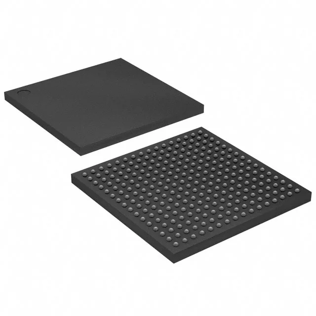
The Intel 10M40DCF484C8G is a MAX® 10 family FPGA delivering 40,000 logic elements and 360 user I/O in a 484-ball BGA package. It integrates non-volatile configuration memory, so it powers up immediately without an external configuration device — a fit for systems that need instant-on operation or simplified BOM. The 1,290,240 bits of embedded RAM handle small FIFOs, register files, or line buffers, reducing external memory count.
Core supply and decoupling
Place bulk and bypass capacitors near each VCC pin group; the 484-BGA land pattern has central balls for core power.
I/O count and package trade-offs
With 360 I/O in a 484-BGA (23x23 mm), this part balances pin density against board-layer count. The sibling 10M40DCF672C7G offers 500 I/O in a larger 672-ball package but requires a more complex PCB with tighter escape routing. For designs that do not need the extra I/O, the 484-BGA saves board area and reduces via congestion.