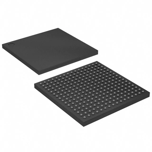
Intel 10M40DAF672C8G — FPGA / CPLD & Programmable Logic

Intel 10M40DAF672C8G MAX 10 FPGA, 40K LE, 500 I/O, 672-FBGA

MPN10M40DAF672C8G
Active

Intel MAX 10 series FPGA, 10M40DAF672C8G, 40,000 logic elements, 500 I/O, 1,290,240 total RAM bits, 1.15V–1.25V supply, 672-FBGA (27x27 mm), commercial temperature 0°C to 85°C, Tray.

$107.7703Ref. price · indicative, final on quote
StockContact for availability
MOQ1 pcs
  • 100% new & originalTraceable channels only — no refurbs, no pulls, no remarked parts.
  • Date & lot codes on quoteStated per line before you commit; label photos on request.
  • MSL-compliant ESD packingMoisture-sealed bags with indicator cards; reels photo-verified.
  • PayPal buyer protectionPay by T/T, PayPal or Payoneer — card payments covered end to end.

Specifications

10M40DAF672C8G Technical Specifications
ParameterValue
SeriesMAX® 10
Mounting typeSurface Mount
Voltage1.15V ~ 1.25V
Operating temperature0°C ~ 85°C (TJ)
PackageTray
Number of i (O)500
Case672-BGA
Total RAM bits1290240
Number of LABs (CLBs)2500
Number of logic elements (Cells)40000

Product details

40,000 logic elements, 500 I/O — what this FPGA delivers

The 500 I/O count differentiates this part from the 10M40DAF484C8G sibling. The commercial temperature grade (0°C to 85°C) suits indoor equipment; the -I grade (10M40DAF672I6G) covers -40°C to 100°C.

672-FBGA — board integration notes

The 672-ball FBGA (27x27 mm) is a fine-pitch BGA. It requires a multi-layer PCB with controlled impedance for the I/O banks. The 500 I/O are distributed across multiple banks with dedicated VCCIO pins. MAX 10 devices support internal configuration flash, eliminating the need for an external configuration memory in many designs. Programming is done via JTAG or through the internal flash controller; the device can also act as a configuration device for other FPGAs in a multi-FPGA system.

Frequently asked questions

What is the difference between 10M40DAF672C8G and 10M40DAF672C7G?

Both parts share the same 40,000 logic elements, 500 I/O, and 672-FBGA package. The 10M40DAF672C7G is a faster speed grade (C7 vs C8), meaning tighter timing margins and higher maximum frequency. If your design is already timing-closed on the C8, the C7 offers headroom; otherwise the C8 is the cost-optimized choice.

What is the exact specification of 10M40DAF672C8G?

The 10M40DAF672C8G is an Intel MAX 10 FPGA with 40,000 logic elements, 500 I/O, 1,290,240 total RAM bits, 2,500 LABs/CLBs, a 1.15V–1.25V supply, commercial temperature range 0°C to 85°C, and a 672-FBGA (27x27 mm) package.

What is the pinout of 10M40DAF672C8G?

The pinout is defined in the Intel MAX 10 device family datasheet and pin connection guidelines. The 672-ball FBGA ball map is available in the official documentation; it is not reproduced in this listing. Verify bank assignments and I/O standards against your schematic before layout.