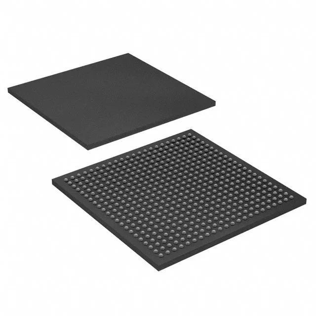
The 10M25DCF484C7G is a MAX® 10 FPGA with 25000 logic elements and 360 user I/O in a 484-FBGA package (23x23 mm). The 25K LE count puts it in the mid-range of the MAX 10 family — enough for a modest sensor fusion engine, a display timing controller, or glue logic consolidation on a single-chip FPGA without external configuration memory (the MAX 10 integrates the flash). The 360 I/O in a 0.8 mm pitch BGA means the fan-out drives the layer count. A 4-layer board can break out the outer two rows; the inner balls need a 6-layer stack-up with blind vias or microvias. The core supply is a single 1.15V to 1.25V rail — one LDO or switching regulator covers it, no multi-rail sequencing.
What the 691200 RAM bits and 1563 LABs buy you
691200 total RAM bits (about 86 KB) is enough for small FIFOs, line buffers for a VGA-resolution display, or coefficient storage for a digital filter. The 1563 LABs/CLBs each contain 10 logic elements, giving 15630 LEs in the logic-array fabric plus the routing and dedicated arithmetic blocks that the MAX 10 architecture adds on top of the LE count. The 0°C to 85°C commercial temperature grade means this part is for indoor equipment — networking gear, industrial HMIs, test equipment in a conditioned environment. Not for under-hood automotive or outdoor base stations without active cooling.