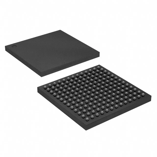
Intel 10M16SCU169A7G — FPGA / CPLD & Programmable Logic

Intel 10M16SCU169A7G MAX 10 FPGA, 16K LE, 130 I/O

MPN10M16SCU169A7G
Active

Intel MAX® 10 FPGA, 10M16SCU169A7G, 16,000 logic elements, 130 I/O, 562176 total RAM bits, 169-LFBGA/UBGA (11x11 mm), -40°C to 125°C, 2.85V–3.465V supply, Tray, RoHS compliant.

$56.1700Ref. price · indicative, final on quote
Packaging169-LFBGA
RoHSRoHS Compliant
SeriesMAX® 10
Independent supplier — new & surplus stockAuthenticity-screened · ESD-safe packingListing updated Aug 2026

Specifications

10M16SCU169A7G specifications
ParameterValue
SeriesMAX® 10
MountingSurface Mount
Voltage2.85V ~ 3.465V
Operating temperature-40°C ~ 125°C (TJ)
PackageTray
Number of i (O)130
Case169-LFBGA
Total RAM bits562176
Number of LABs (CLBs)1000
Number of logic elements (Cells)16000

Product details

Logic density and I/O budget for glue-logic integration

The 10M16SCU169A7G packs 16,000 logic elements into the MAX 10 family — enough to absorb a handful of 8-bit state machines, a UART or SPI bridge, and a small video timing controller without reaching for a larger device. 130 user I/O in a 169-ball BGA means roughly 77% of the balls are signal pins; the rest are supply and ground. That I/O count supports a 16-bit data bus plus address and control lines to an external SRAM or ADC, with room left for a parallel LCD interface. The 562,176 bits of embedded RAM (about 549 Kbit) can hold a 640×480 pixel frame buffer at 1-bit depth, or serve as a dual-clock FIFO for crossing clock domains between a fast ADC and a slower MCU bus.

Supply rail and temperature grade for industrial deployment

A single 2.85 V to 3.465 V supply rail powers the core and I/O banks — no separate VCCINT and VCCIO regulators are needed, which simplifies the power tree to one 3.3 V rail and a handful of decoupling caps per the layout guide. The A7 speed grade is the industrial-temperature variant; the C8 grade (0°C to 85°C) is the commercial sibling.

Package footprint and board-level integration

The 169-ball LFBGA (also marked as 169-UBGA) measures 11×11 mm with a 0.8 mm ball pitch. That pitch is fine enough to require a 4-layer board for fan-out — two-layer designs will struggle to route all 130 I/O without via stubs or necked traces. If the bake history is unknown, a 24-hour bake at 125°C before reflow is cheap insurance against popcorning.

RoHS compliant per the listing — no lead in the solder balls or package finish, which clears EU and Chinese regulatory requirements without an exemption.

Frequently asked questions

What are the key electrical specifications of 10M16SCU169A7G?

The package is a 169-ball LFBGA/UBGA (11×11 mm, 0.8 mm pitch).

Is 10M16SCU169A7G RoHS compliant?

Yes, the listing confirms RoHS compliance. No lead or restricted substances above the threshold limits.

What is the difference between 10M16SCU169A7G and 10M08SCU169A7G?

The 10M16 has 16,000 logic elements and 562,176 RAM bits, while the 10M08 has approximately 8,000 logic elements and 387,072 RAM bits. Both share the same 169-UBGA package and 130 I/O count. The 10M16 is the higher-density sibling for designs that need more logic or memory.

What is the closest functional second-source for 10M16SCU169A7G?

The 'A' in the suffix indicates the commercial/industrial speed grade; the 'C' in the SCU variant denotes the extended temperature range. Both are pin-compatible in the same 169-UBGA footprint.