Logic density and I/O budget for a glue-logic FPGA
The 10M08DAF256A7G packs 8000 logic elements (500 LABs/CLBs) and 387072 bits of embedded RAM — enough to absorb a moderate state machine, a few SPI/I2C bridges, and a small frame buffer without reaching for a larger die. 178 user I/O in a 256-ball FBGA means roughly 70% of the balls are signal — the rest are supply and ground. That ratio supports a wide parallel bus (e.g., an 8- or 16-bit LCD interface) alongside serial peripherals, but the 17x17 mm footprint limits the number of differential pairs you can route before the escape vias crowd the inner rows.
The single 1.2V nominal core rail simplifies the power tree: a small LDO or a buck converter feeding the VCCINT plane, with the I/O banks taking their own 3.3V or 2.5V from a separate regulator. No multiple core voltages to sequence.
Package and board integration
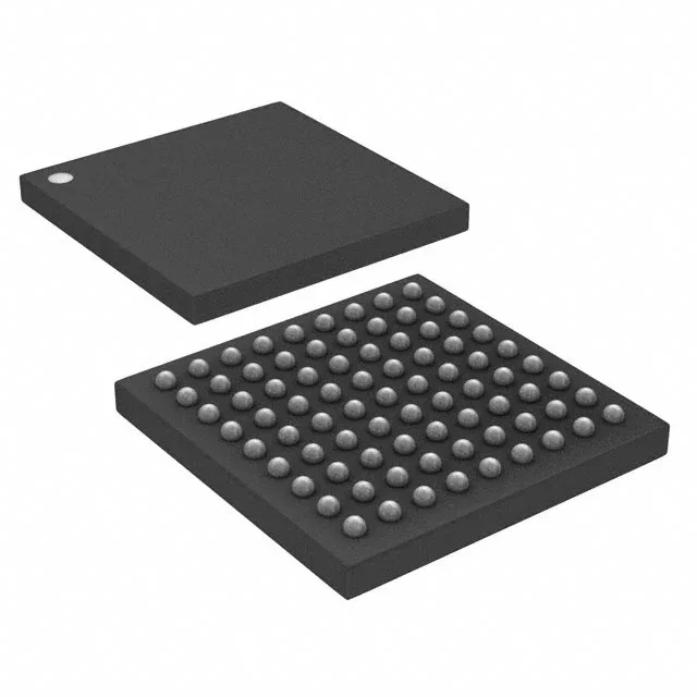
256-ball FBGA, 17x17 mm body, 1.0 mm ball pitch — four-layer board is sufficient for fan-out if you stagger the via-in-pad on the inner rows. The 0.8 mm ball diameter gives decent solder-joint standoff for rework under X-ray inspection. Surface-mount only, supplied in tray — no tape-and-reel option listed, so volume pick-and-place requires a tray feeder or a bulk-to-tape conversion. The 256-LBGA package code matches the standard JEDEC MO-216 footprint.