12V rail transient suppression — how the clamping chain works
The 1.5SMCJ12A-AQ: The 12V reverse standoff is the working voltage the diode expects in normal operation — it sits reverse-biased on a 12V rail and does not conduct. When a load dump or inductive kickback drives the line above 13.3V, the Zener avalanche kicks in and the device enters its clamping region. The maximum clamping voltage under the peak impulse is 19.9V at a peak pulse current of 75.4A (10/1000µs waveform). 19.9V at 75.4A is the ceiling the downstream circuitry must survive — the downstream IC's abs-max rating must be above 19.9V with enough margin that the clamping event does not erode lifetime. The 1500W peak pulse rating gives the diode the energy-handling margin for automotive ISO 7637-2 style transients without degradation. Power line protection is listed as No — this is a signal-line or local rail clamp, not a bus protector designed for repeated fault-current interruption on a mains rail.
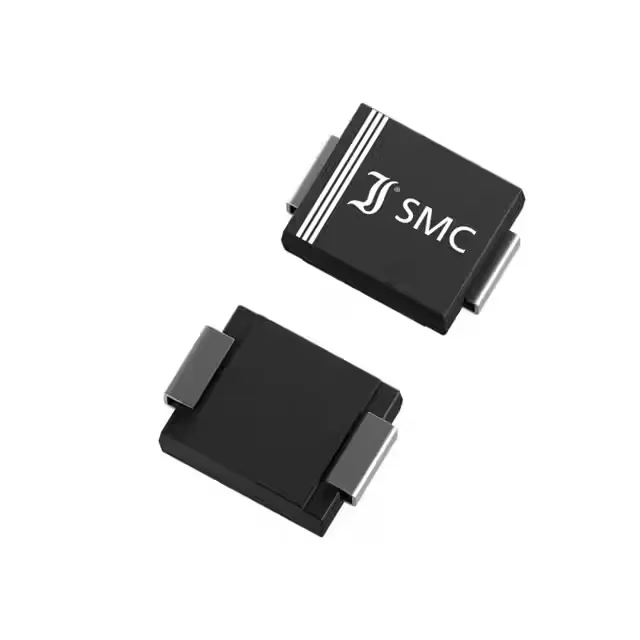
SMC footprint and thermal management for the board layout
The DO-214AB (SMC) package has a thermal pad under the cathode tab that must be soldered to a properly sized land pattern for effective heat sinking to the board copper. The junction-to-ambient thermal resistance is governed by the pad area and via count — under-size the pad and the clamping event drives the junction above the 150°C rated ceiling. Operating junction range is −50°C to +150°C — the automotive ambient range in an engine bay or chassis module leaves headroom above the 85°C typical in those environments, but check the thermal pad design against the diode's power derating curve if the clamping event duty cycle is non-trivial.