Dual op-amp for signal conditioning up to 5 MHz
The LT1492CS8#TRPBF is a dual general-purpose operational amplifier from the Analog Devices LT® series, packing a 5 MHz gain-bandwidth product and a 3 V/µs slew rate into the 8-SOIC footprint. With two independent channels drawing 425 µA each, it fits signal-conditioning stages where moderate bandwidth and low quiescent current are the constraints — think anti-aliasing filters, sensor buffers, or active loops in industrial control or test equipment.
Supply range and temperature grade
The supply span runs from 2.5 V to 36 V, single or split, covering common 3.3 V, 5 V, ±5 V, and ±15 V rails without needing a separate regulator. The operating temperature range is 0°C to 70°C — commercial grade, so the part is intended for indoor, temperature-controlled environments rather than automotive or extended industrial bays. Input offset voltage is 120 µV typical, and input bias current is 50 nA — adequate for precision work with moderate source impedances, though a JFET-input op-amp would be a better fit for high-impedance sensors above 100 kΩ.
Output drive and quiescent budget
Each channel can source or sink 55 mA, enough to drive a 100 Ω load to ±5.5 V or to charge the input capacitance of a successive-approximation ADC in a single settling time constant. The 425 µA per-channel supply current keeps the total quiescent draw under 1 mA for both amplifiers — a comfortable fit for multi-channel, battery-powered or thermally constrained designs.
Package and mounting
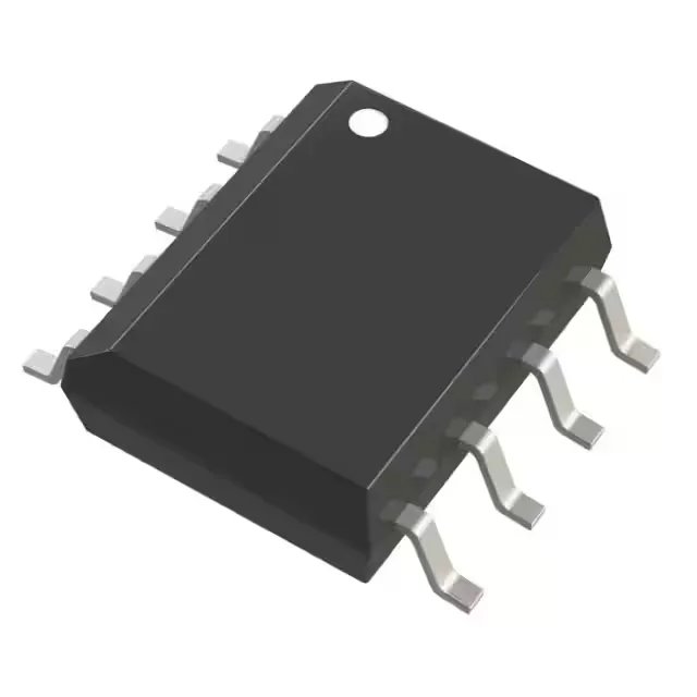
Housed in an 8-SOIC package with 3.90 mm body width (supplier device package 8-SO), the part is a drop-in for standard SO-8 land patterns. Surface-mount only — no through-hole variant. Supplied on Tape & Reel, also available as Cut Tape for prototype quantities.
Lifecycle and compliance
Analog Devices lists the LT1492CS8#TRPBF as Active in production. The part is ROHS3 compliant, so no exemption-based paperwork is needed for EU or California market shipments.