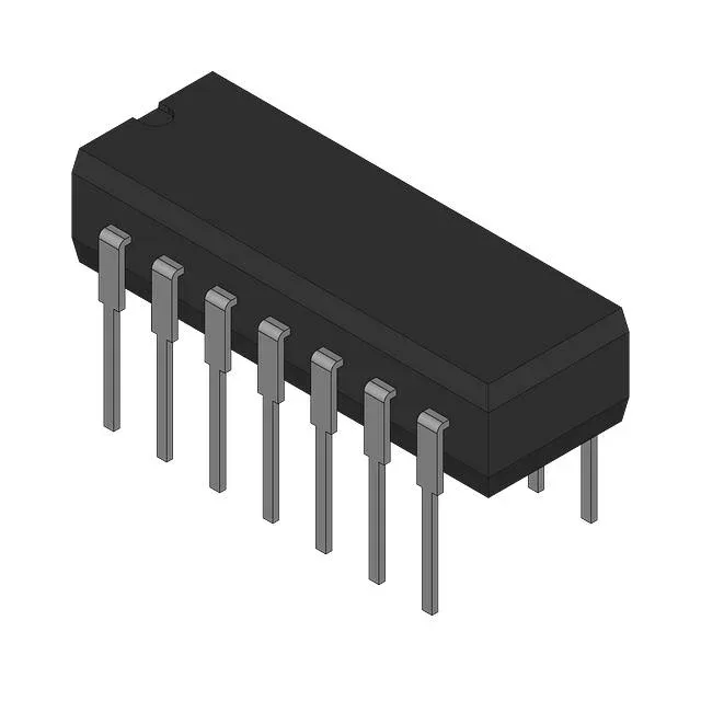
Analog Devices AD5539JQ — Logic ICs

AD5539JQ General Purpose Op-Amp, 600 V/µs Slew Rate

MPNAD5539JQ
End of Life

Analog Devices AD5539JQ, General Purpose Amplifier, 1 Circuit, 14-CDIP (0.300", 7.62mm), Through Hole, 600 V/µs Slew Rate, 1.4 GHz Gain Bandwidth, 14 mA Supply, 0°C to 70°C.

$6.0Ref. price · indicative, final on quote
Packaging14-CDIP (0.300", 7.62mm)
StockContact for availability
MOQ1 pcs
  • 100% new & originalTraceable channels only — no refurbs, no pulls, no remarked parts.
  • Date & lot codes on quoteStated per line before you commit; label photos on request.
  • MSL-compliant ESD packingMoisture-sealed bags with indicator cards; reels photo-verified.
  • PayPal buyer protectionPay by T/T, PayPal or Payoneer — card payments covered end to end.

Specifications

AD5539JQ Technical Specifications
ParameterValue
Mounting typeThrough Hole
Amplifier typeGeneral Purpose
Voltage - input offset2 mV
Voltage - supply span20 V
Current - supply14mA
Current - input bias6 µA
Operating temperature0°C ~ 70°C
Gain bandwidth product1.4 GHz
PackageBulk
Slew rate600V/µs
Case14-CDIP (0.300\", 7.62mm)
Number of circuits1

Product details

14-pin CERDIP — hermetic, through-hole, RoHS-exempt

The AD5539JQ is a single-channel general-purpose op-amp from Analog Devices, packaged in a 14-lead CERDIP (0.300" body) with through-hole mounting. The hermetic ceramic package suits environments where moisture resistance or high-temperature storage is required, and the through-hole format keeps it compatible with socketed or legacy PCB layouts.

With a slew rate of 600 V/µs and a gain-bandwidth product of 1.4 GHz, this amplifier is built for high-speed pulse amplification, video distribution, or RF front-end stages where settling time and large-signal bandwidth matter.

Supply range and input offset — 9 V to 20 V, 2 mV max

The supply span runs from 9 V minimum to 20 V maximum, allowing operation on ±5 V to ±10 V dual rails or a single 12 V or 15 V rail. Input offset voltage is specified at 2 mV, and input bias current at 6 µA — both typical for a high-speed bipolar input stage. These numbers are not precision-grade, so the part is better suited to AC-coupled or closed-loop gain stages than DC-accurate instrumentation paths.

Active lifecycle, RoHS non-compliant — sourcing notes

However, it is marked RoHS non-compliant — the hermetic CERDIP package uses lead-based solder seals or tin-lead plating, which exempts it from RoHS restrictions in many military, aerospace, and medical applications but blocks it from EU RoHS-compliant BOMs.

Frequently asked questions

What are the best alternatives to AD5539JQ?

A close functional peer is the AD827JNZ, a dual-channel op-amp in a through-hole PDIP with a 300 V/µs slew rate and 50 MHz bandwidth — half the slew rate of the AD5539JQ but in a dual package. For a single-channel surface-mount alternative, the AD847JRZ-REEL7 offers 300 V/µs slew rate in an SOIC package. Neither is a pin-for-pin replacement; the AD5539JQ's 600 V/µs slew rate and 1.4 GHz GBP remain unique in this package family.