What the MEMS resonator changes for your clock tree
The ASEMB-33.330MHZ-LR is a CMOS-output XO (Standard) using a MEMS resonator rather than an AT-cut crystal — the base resonator entry lists MEMS as the source. This shifts the shock and vibration profile decisively: MEMS resonators have no piezoceramic fracture risk and maintain frequency under mechanical stress that would stress-grain a crystal. For portable or industrial equipment where the board sees >50 g shock, the MEMS base is the primary selection driver, not a footnote. The tradeoff is that MEMS oscillators typically carry slightly higher phase noise floor than high-Q crystal XOs at offsets beyond 1 MHz — if the 33.33 MHz clock feeds a PLL or clock cleaner, verify the phase-noise mask against the MEMS plot before committing the BOM line.
33.33 MHz and the supply rails — what fits this clock
The 33.33 MHz frequency is a non-trivial clock choice — 33.333... MHz is the 5th submultiple of the 166.666... MHz USB High-Speed reference, and it also appears as a divide-down target in Ethernet PHY clock trees and some CAN FD designs. The ±25ppm frequency stability meets Ethernet 100BASE-TX tolerance (±50 ppm total) and satisfies most UART and sensor bus clock requirements without a trim register.
Standby pin and the power budget
The standby (power-down) function is the key power-management feature on this part. When asserted, the oscillator draws ≤15 µA maximum, compared to 16 mA maximum in normal operation — roughly a 1000× reduction. A battery-powered node that needs the clock only during active sampling or burst transmission can gate the ASEMB rather than letting a continuously-running crystal oscillator burn 16 mA between events. The 15 µA disable figure is the floor to design against; the actual current in a powered-off state is what the downstream logic sees as load, so verify the upstream rail can tolerate that residual draw if the supply stays energized during standby.
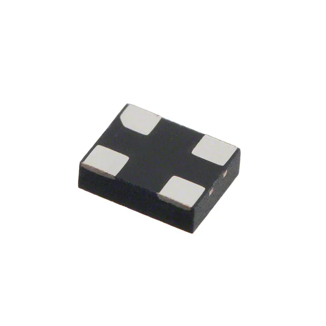
Footprint and the 3.2 × 2.5 mm package for dense layouts
The ultra-low profile makes it viable under daughtercards or alongside tall connectors; the no-lead frame calls out a thermal pad land pattern — confirm the layout uses the manufacturer-recommended landing pad and solder mask opening, because MEMS oscillator paste reflow profiles are more sensitive to voiding than standard crystal packages. Standard surface-mount pick-and-place handling applies — no special co-planarity concerns with this package style.