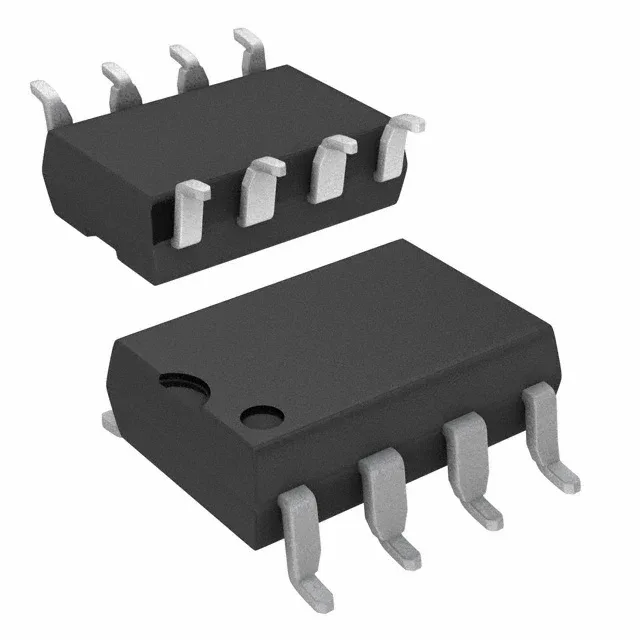
Toshiba Semiconductor TLP352(D4-TP1,F) — Power Management (PMIC / Gate Driver)
Technical Documents PDF / CAD
RoHS Compliant · Lead-Free EIA-481 Standard
Toshiba Semiconductor / Power Management (PMIC / Gate Driver)

Toshiba TLP352(D4-TP1,F) Gate Drive Optocoupler, 3750Vrms

MPN TLP352(D4-TP1,F)
End of Life Spot Stock · 24-48h Dispatch 100% Original Sealed

Toshiba TLP352(D4-TP1,F) optical coupling gate driver, 1 channel, 3750Vrms isolation, 2.5A peak output, 15V~30V supply, 8-SMD gull wing, -40°C~125°C.

In Stock: 19,738 pcs
MOQ: 1 pcs
Logistics: DHL / FedEx DAP (Global Express · 3-7d) Russia & CIS DDP (Door-to-Door Cleared)
Dispatch: Shenzhen / HK
Unit Price (USD)
$1.95 / pc
Direct Purchase Ready
Volume Pricing Breaks Confirmed upon quotation
1+ pcs
$1.95
10+ pcs
$1.76
30+ pcs
$1.60
100+ pcs
$1.44
500+ pcs
$1.35
1,000+ pcs
$1.27
Working on a production BOM or have a target unit price? Submit Target Price
Buy Now

$1.95 / ea

19,738 in stock — maximum per order · 3–4 days lead time

$1.76 / ea from 10 pcs

Upload Full BOM List
[SPEC] Essential Parameters Snapshot Full Specifications (17)
Package / Case 8-SMD, Gull Wing
Output / Current 2A, 2A
ALT
Facing long factory lead times or allocation on TLP352(D4-TP1,F)? Verified pin-compatible alternatives available with active Shenzhen stock and 100% solder-ready footprint match.

Full Technical Specifications

17 Parameters
TLP352(D4-TP1,F) specifications
Parameter / AttributeSpecification / Value
MountingSurface Mount
Voltage - isolation3750Vrms
Voltage - output supply15V ~ 30V
Voltage - forward (Vf)1.55V
Current - peak output2.5A
Current - output high, low2A, 2A
Current - DC forward (If)20 mA
Operating temperature-40°C ~ 125°C
Pulse width distortion50ns
Approval agencyCSA, cUL, UL, VDE
PackageTape & Reel (TR); Cut Tape (CT)
TechnologyOptical Coupling
Case8-SMD, Gull Wing
Channels1
Rise (Fall time)15ns, 8ns
Propagation delay tpLH (tpHL)200ns, 200ns
Common mode transient immunity20kV/µs
100% Footprint Match · Solder-Ready (No PCB Redesign Needed)

Need Stock or a Drop-in Second-Source for TLP352(D4-TP1,F)?

Package: DIP-8 (gate-drive optocoupler) · Pin-compatible replacements with immediate Shenzhen spot stock

Footprint Match 97%
Supply Chain & Allocation Reality:

This eight-pin row is how inverter, servo and welder drive boards cross the isolation barrier to fire their IGBTs: TLP250 from Toshiba, HCPL-3120/A3120 from the Avago lineage, FOD3120 from the Fairchild line - four houses, one socket, and a repair literature that swaps them by name. The selection axis is output current (TLP250 at a 1.5A peak against the 2.5A class of its successors) and input threshold (the 3120 triggers from a lower LED current), and the design axis is the negative gate rail that keeps Miller capacitance from re-triggering the IGBT. In repair, the row behaves; what re-fails is the rail and the bypass capacitor the procedure keeps forgetting.

Verified Pin-Compatible Replacements (3 verified alternatives)

TLP350 Toshiba DIP-8
100% Drop-in (Zero Code Change)
Availability & Target Pricing:

The Documented Upgrade in the Same Socket

Shenzhen Spot Stock (24-48h Dispatch)

Electrical & Core Specs:

The higher-output member: about +/-2.5A peak against the TLP250s +/-1.5A, aimed at 1200V IGBTs in the 20-100A class, with lower supply current - the direct upgrade path of the row.

Gate-side supply in the 10-35V class; isolation 2500V class.

Compatibility & Drop-In Notes: The substitution rule reported from inverter repair: in low-power drives the smaller part can stand in for the bigger; in mid and high-power drives the output current difference matters, although many designs carry a post-amplifier stage that softens it.
Package & Solder Footprint: Standard 8-pin gate-drive optocoupler pinout across the row.
Shenzhen Warehouse Stock & MOQ: Active Toshiba line; the forward part of the socket.
HCPL-3120 Broadcom (Avago) DIP-8
Functional Equivalent
Availability & Target Pricing:

The Other House of the Same Socket

Shenzhen Spot Stock (24-48h Dispatch)

Electrical & Core Specs:

The Avago-line drive optocoupler: about +/-2A output, direct drive of 150A/1200V IGBT modules, and a lower LED threshold (about 2.5mA) that changes the input-side resistor arithmetic.

15V to 30V gate-side supply; isolation 1414V class (the HCNW variant carries the higher figure).

Compatibility & Drop-In Notes: The input-current difference is the practical one when crossing houses: a drive resistor sized for the 250s 5mA can overdrive a 3120s LED budget - and the reverse starves. Recompute the input resistor, then treat the row as interchangeable.
Package & Solder Footprint: Same 8-pin socket; the HCNW3120 is electrically the same part in a wider isolation body.
Shenzhen Warehouse Stock & MOQ: Multi-line stock; the standard alternative of the drive-repair trade.
FOD3120 onsemi (Fairchild line) DIP-8
100% Drop-in (Zero Code Change)
Availability & Target Pricing:

The Fairchild-Line Member

Shenzhen Spot Stock (24-48h Dispatch)

Electrical & Core Specs:

The Fairchild-line drive optocoupler with the 2.5A-class output: functionally the TLP350 of the row in the onsemi lineage.

Same gate-side envelope as the row.

Compatibility & Drop-In Notes: The row rule applies: verify the input threshold figure of the exact member, recompute the LED resistor if crossing houses, and treat output current as the power-class decision.
Package & Solder Footprint: Standard 8-pin pinout.
Shenzhen Warehouse Stock & MOQ: Stocked with the row; the documented second source for A3120 designs.
Buyer & Quality Checklist for Sourcing Alternatives
  • The negative gate rail is the design, not the luxury: a VEE below emitter (the +15/-15V or +15/-8V schemes) prevents Miller-capacitance false turn-on in bridge drives. Repairs that skip the negative rail reintroduce the shoot-through the original design existed to avoid.
  • The bypass capacitor lives between pins 8 and 5 (0.1uF class) - it is in every application note and on no repair checklist; missing it turns switching transients into mysterious drive glitches.
  • Crossing houses recomputes the input resistor: Toshiba members trigger around 5mA, the 3120 family around 2.5mA - the difference is the LED and eventually the driver behind it.
  • Output current is the power-class axis: 1.5A against 2.5A peaks decides whether the part drives the IGBT gate directly or leans on a post-amplifier stage - read the schematic, not the name.
  • When a drive optocoupler fails, the IGBT usually failed first (or together): meter the gate-emitter junction and the collector path before fitting the third driver into the same board.
  • In repair inventory, the row is one drawer with one trap: isolation grade differences (HCNW and wide-body variants) mean the subs that exist on paper are not always subs on the board.
Frequently Asked Technical Questions

Q: Can TLP250 and HCPL-3120 replace each other?

A: In low-power drives yes - the reported practice is direct interchange in the 8-pin socket - with the input-resistor recomputation for the different LED thresholds (about 5mA against 2.5mA). In mid and high-power drives compare the output-current class first.

Q: What drives TLP250 output current selection?

A: The IGBT gate charge and the absence of a post-amplifier stage: 1.5A peaks suit the 50A/1200V class the TLP250 was specified for, while the 2.5A members (TLP350, FOD3120) cover 20-100A modules without help.

Q: Why do repaired inverter drives fail again at power-up?

A: Commonly the negative gate rail or the missing bypass capacitor: without VEE the Miller capacitance false-triggers the bridge, and without the 0.1uF at pins 8-5 the drive sees every switching transient. Check both before blaming the new optocoupler.

Technical Details & Description

Gate-drive optocoupler for IGBT/MOSFET switching

The Toshiba TLP352(D4-TP1,F) is a single-channel optical coupling gate driver designed to drive IGBTs and power MOSFETs in isolated switch-mode power supplies, motor drives, and inverter stages. It delivers 2.5A peak output current with 2A symmetrical sink and source capability, enough to charge and discharge the gate of a medium-power IGBT without an external booster stage. The 3750Vrms isolation rating and 20kV/µs common-mode transient immunity (CMTI) let it sit on the secondary side of the isolation barrier while the primary-side controller commands switching events — the CMTI figure is the one that matters when the power stage commutates at high dv/dt and you need the driver to stay latched, not glitch the gate. Supply voltage range of 15V to 30V covers the typical gate-drive rails for silicon IGBTs and standard MOSFETs; the 1.55V typical forward voltage on the LED input side lets it interface directly with 3.3V or 5V logic through a series resistor.

3750Vrms isolation — where the barrier holds

The 3750Vrms isolation voltage is a reinforced-single-insulation rating suitable for mains-isolated applications up to 300V working voltage in pollution degree 2 environments. The 8-SMD gull-wing package with 8 mm creepage between input and output sides supports the clearance needed for safety-agency compliance. Approvals from CSA, cUL, UL, and VDE mean the part carries the marks accepted in North American and European safety-certified designs — no additional qualification testing for the isolation barrier in most industrial and commercial power supplies.

Switching timing and drive strength

The 50ns maximum pulse-width distortion means the on-time and off-time skew between input and output stays tight — relevant when you are paralleling multiple drivers and need matched gate signals. The 2.5A peak output rating is the headline number for driving the gate charge; the 2A symmetrical high/low current tells you the sink and source paths are balanced, so the turn-off speed matches the turn-on speed without extra gate-resistor asymmetry.

The 20 mA maximum LED forward current is the limit to watch when driving the input side from a logic output — size the series resistor to keep the LED current well below that ceiling across the temperature range.

Frequently asked questions

Is TLP352(D4-TP1,F) compatible with 15V gate drive?

Yes. The output supply range is 15V to 30V, so a 15V gate-drive rail is within the operating window. The 2.5A peak output at 15V supply still provides enough gate charge to switch a standard IGBT or MOSFET at moderate frequency.

What is the difference between TLP352 and TLP350?

The TLP352 family offers higher peak output current (2.5A versus the TLP350's lower rating) and faster switching with 15ns/8ns rise/fall times. The TLP350 is an older generation with slower propagation delays and lower CMTI. For new designs driving medium-power IGBTs, the TLP352 is the preferred choice.

TLP352(D4-TP1,F)
Verified Allocation
Quote