Toshiba Semiconductor TCR3UG25A,LF — Discrete Semiconductors

Toshiba TCR3UG25A,LF LDO, 300mA, 2.5V Fixed, 4-WCSP-F

MPNTCR3UG25A,LF
End of Life

Toshiba Semiconductor TCR3UG series LDO regulator, TCR3UG25A,LF, 300mA output, 2.5V fixed, 680nA quiescent, 70dB PSRR at 1kHz, 4-WCSP-F package.

$0.46Ref. price · indicative, final on quote
Packaging4-XFBGA, WLCSP
StockIn Stock (19)
Lead timeIn Stock wk
MOQ1 pcs
  • 100% new & originalTraceable channels only — no refurbs, no pulls, no remarked parts.
  • Date & lot codes on quoteStated per line before you commit; label photos on request.
  • MSL-compliant ESD packingMoisture-sealed bags with indicator cards; reels photo-verified.
  • PayPal buyer protectionPay by T/T, PayPal or Payoneer — card payments covered end to end.

Specifications

TCR3UG25A,LF Technical Specifications
ParameterValue
SeriesTCR3UG
Output typeFixed
Mounting typeSurface Mount
Voltage - input5.5V
Voltage dropout0.327V @ 300mA
Voltage - output (Min (Fixed))2.5V
Current - output300mA
Current - quiescent680 nA
Operating temperature-40°C ~ 85°C (TJ)
PSRR70dB (1kHz)
PackageTape & Reel (TR); Cut Tape (CT)
Case4-XFBGA, WLCSP
Control featuresEnable
Protection featuresInrush Current, Over Current, Thermal Shutdown
Number of regulators1
Output configurationPositive

Product details

300 mA LDO with 680 nA quiescent — the battery-life spec

The Toshiba TCR3UG25A,LF is a fixed-output 2.5 V LDO regulator rated for 300 mA continuous output. Its standout number for battery-powered or always-on loads is the 680 nA quiescent current — that is the current the regulator itself draws just to stay alive, and at sub-microamp levels it barely registers against the self-discharge of a lithium cell.

Dropout and protection — what the 0.327 V max means

Maximum dropout voltage is 0.327 V at 300 mA load. Protection features include inrush current limiting, over-current, and thermal shutdown — the regulator handles start-up into a discharged capacitor without the output overshooting, and folds back or shuts down if the load exceeds the rating or the die temperature crosses the threshold. The enable pin lets the system power down the regulator completely — when pulled low, the output goes to high-impedance and the quiescent current drops to near zero, which is useful for sequencing rails or saving power in a sleep state.

Package and temperature — board-fit notes

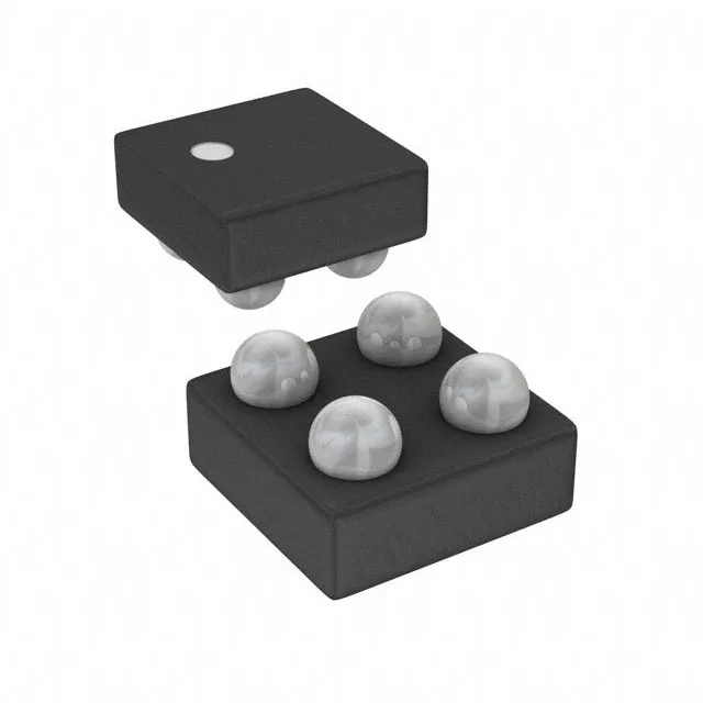
Housed in a 4-XFBGA, WLCSP package (4-WCSP-F, 0.65 x 0.65 mm footprint). This is a wafer-level chip-scale package — no plastic overmold, the die backside is the top of the package. The small footprint saves board area but the solder balls are under the die, so the PCB land pattern must match the Toshiba recommended layout exactly; a 0.35 mm ball pitch demands careful solder-paste stencil design. The package itself is surface-mount and RoHS3 compliant per the lifecycle record.

The part is a single-source LDO — no pin-compatible second-source is listed. The closest functional sibling in the same TCR3UG series is the TCR3UG25B,LF, which shares the same output voltage, current rating, quiescent current, and package; the difference is in the output voltage tolerance or ordering code suffix, not the parametric fit.

Frequently asked questions

What is the PSRR of the TCR3UG25A,LF?

The TCR3UG25A,LF lists a PSRR of 70 dB at 1 kHz. This means ripple on the input rail is attenuated by a factor of roughly 3,000 at that frequency — a 10 mVpp switching ripple becomes about 3 µVpp at the output.

Will the TCR3UG25A,LF drop into a board designed for the TCR3UG25B,LF?

Yes, the TCR3UG25B,LF is the closest functional sibling in the same TCR3UG series. Both share the same 2.5 V output, 300 mA rating, 680 nA quiescent current, and 4-WCSP-F package. The difference is in the ordering code suffix — the B variant may carry a different output voltage tolerance band. Confirm the tolerance requirement against the BOM before substituting.