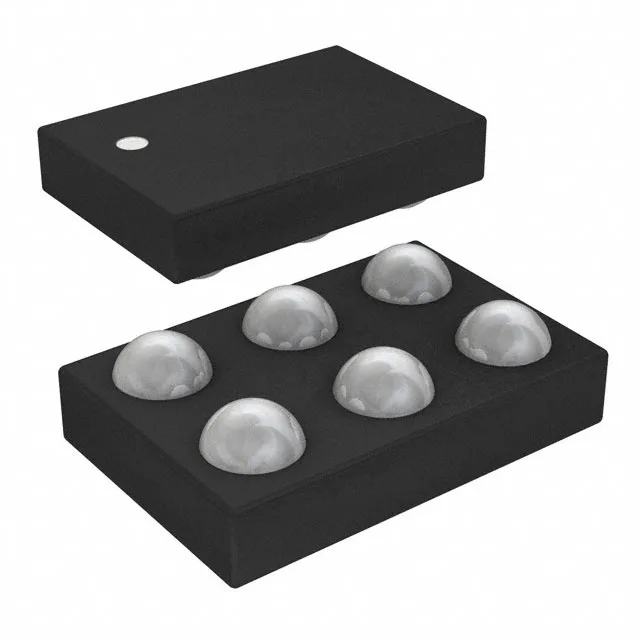
The Toshiba TCR13AGADJ,LF is a 1.3 A positive-output linear regulator in a 6-bump WLCSP (1.2 x 0.80 mm). It belongs to the TCR13AG series and is specified for surface-mount assembly. Maximum dropout is 163 mV at 1 A output — the input rail must stay at least that far above the set output voltage across the load range, or the regulator drops out of regulation. With a 3.3 V input and a 2.8 V output, the 500 mV headroom clears this by a wide margin.
Adjustable output, protection, and quiescent draw
Output voltage is adjustable from a 0.55 V minimum to a 3.6 V maximum, set by an external resistor divider. A single regulator covers sub-1 V core rails up to 3.3 V I/O rails without changing the BOM's regulator IC. Quiescent current is 92 µA typical — low enough that the regulator's own draw does not dominate the battery budget in a portable device that spends most of its time in a light-load state. On-chip protection includes inrush current limiting, over-current shutdown, thermal shutdown, and undervoltage lockout. The UVLO prevents the output from powering up until the input rail is high enough to keep the pass device in its safe operating area.
Package, temperature grade, and compliance
The 6-XFBGA WLCSP package (1.2 x 0.80 mm body) is a wafer-level chip-scale package with six bumps. The land pattern is the bump array itself — no lead frame, no mould compound. Layout must match the 0.40 mm bump pitch typical of this class; the board's solder-mask-defined pads and the stencil aperture control the standoff height. Lifecycle status is active with RoHS3 compliance.