Toshiba Semiconductor TCK22971G,LF — Discrete Semiconductors

TCK22971G,LF Toshiba P-Channel Load Switch, 2A, WLCSP

MPNTCK22971G,LF
End of Life

Toshiba Semiconductor TCK22971G,LF, P-Channel load switch, 1:1 input-output, 2A max output, 25mOhm Rds(on), 1.1V-5.5V load, slew rate controlled, WLCSP-6, Tape & Reel.

$0.54Ref. price · indicative, final on quote
Packaging6-UFBGA, WLCSP
StockIn Stock (14)
Lead time3-5 Days wk
MOQ1 pcs
  • 100% new & originalTraceable channels only — no refurbs, no pulls, no remarked parts.
  • Date & lot codes on quoteStated per line before you commit; label photos on request.
  • MSL-compliant ESD packingMoisture-sealed bags with indicator cards; reels photo-verified.
  • PayPal buyer protectionPay by T/T, PayPal or Payoneer — card payments covered end to end.

Specifications

TCK22971G,LF Technical Specifications
ParameterValue
Input typeNon-Inverting
Output typeP-Channel
Switch typeGeneral Purpose
Mounting typeSurface Mount
Voltage - load1.1V ~ 5.5V
Voltage - supply (Vcc (Vdd))Not Required
Current - output2A
Number of outputs1
InterfaceOn/Off
Operating temperature-40°C ~ 85°C (TA)
PackageTape & Reel (TR); Cut Tape (CT)
FeaturesSlew Rate Controlled
Rds on25mOhm
Case6-UFBGA, WLCSP
Fault protectionReverse Current
Output configurationHigh Side
Ratio - Input:Output1:1

Product details

Load switch for battery-powered portable gear

The TCK22971G,LF is a single-channel, high-side P-Channel load switch from Toshiba, designed to enable or disable power rails in portable electronics where board space is tight and on-resistance matters. It handles up to 2 A continuous output across a load voltage range of 1.1 V to 5.5 V, with a typical Rds(on) of 25 mOhm — low enough that at 2 A the conduction loss stays under 100 mW, so the WLCSP package doesn't need a copper pour to stay cool. The switch is controlled by a simple On/Off logic input (non-inverting), and no external Vcc supply is required — the gate drive is derived from the load rail itself.

Slew-rate control and reverse-current blocking

Slew rate controlled switching means the output voltage ramps up gradually when the enable pin goes high — this limits inrush current into downstream decoupling caps and prevents the upstream rail from dipping during power-up. Built-in reverse current protection blocks current flow from the output back to the input when the switch is off, which is useful in multi-rail systems where one rail might stay live while another is gated.

WLCSP-6 package — board-fit considerations

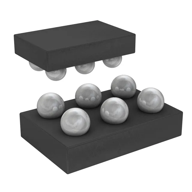
The device comes in a 6-bump WLCSP (0.80 x 1.2 mm body) — the 0.4 mm pitch and exposed bumps mean the PCB land pattern must match the Toshiba recommended footprint exactly to avoid solder bridging and ensure reliable contact. Because it's a wafer-level chip-scale package, the MSL rating is typically MSL-1 (no moisture sensitivity bake required before reflow), but verify the reel label — if it's MSL-3 or higher, bake it before the oven or it popcorns.

Frequently asked questions

What is the closest functional second-source to TCK22971G,LF?

The TCK22972G,LF is a functional peer with the same 25 mOhm Rds(on), 2 A output, and WLCSP-6 package — the key difference is the output configuration (high side vs P-Channel) and the specific enable logic. The TCK22971G,LF uses a non-inverting input and P-Channel output, while the TCK22972G,LF shares the same high-side topology. Verify the enable polarity and output type against your schematic before substituting.