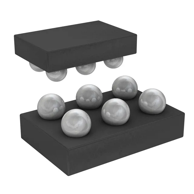
Toshiba Semiconductor TCK22925G,LF — Discrete Semiconductors

Toshiba TCK22925G,LF P-Channel Load Switch, 2A, 25mOhm

MPNTCK22925G,LF
End of Life

Toshiba Semiconductor TCK22925G,LF P-Channel High-Side Load Switch, 2A max output, 25mOhm Rds(on) typ, 1.1V-5.5V load, 6-UFBGA WLCSP package, Tape & Reel.

$0.49Ref. price · indicative, final on quote
Packaging6-UFBGA, WLCSP
StockIn Stock (24)
Lead timeIn Stock wk
MOQ1 pcs
  • 100% new & originalTraceable channels only — no refurbs, no pulls, no remarked parts.
  • Date & lot codes on quoteStated per line before you commit; label photos on request.
  • MSL-compliant ESD packingMoisture-sealed bags with indicator cards; reels photo-verified.
  • PayPal buyer protectionPay by T/T, PayPal or Payoneer — card payments covered end to end.

Specifications

TCK22925G,LF Technical Specifications
ParameterValue
Input typeNon-Inverting
Output typeP-Channel
Switch typeGeneral Purpose
Mounting typeSurface Mount
Voltage - load1.1V ~ 5.5V
Voltage - supply (Vcc (Vdd))Not Required
Current - output2A
Number of outputs1
InterfaceOn/Off
Operating temperature-40°C ~ 85°C (TA)
PackageTape & Reel (TR); Cut Tape (CT)
FeaturesLoad Discharge, Slew Rate Controlled
Rds on25mOhm
Case6-UFBGA, WLCSP
Fault protectionReverse Current
Output configurationHigh Side
Ratio - Input:Output1:1

Product details

What this switch does on your rail

The TCK22925G,LF is a single-channel P-channel high-side load switch from Toshiba, rated for 2 A continuous output across a 1.1 V to 5.5 V load voltage range. The 25 mOhm typical Rds(on) keeps conduction losses low — at 2 A the dissipation is about 100 mW, well within the WCSP6E package's thermal budget at 85°C ambient. It integrates a slew-rate controlled turn-on to limit inrush current into capacitive loads, plus reverse-current blocking when the output voltage exceeds the input — the scorch mark on a board trace tells you when that protection was missing.

Housed in a 6-ball WLCSP (6-UFBGA, supplier package 6-WCSPE 0.80x1.2), this is a fine-pitch BGA-style package. The 0.80 mm x 1.2 mm footprint demands a controlled solder-paste stencil and a reflow profile suited to lead-free assemblies — no hand-soldering this one. Surface-mount only. The On/Off interface is non-inverting and requires no external Vcc supply — the switch is self-biased from the load rail, saving a pin on the upstream regulator.

Frequently asked questions

How do I get current pricing and availability for TCK22925G,LF?

This part is sourced to order through independent distribution. Submit an RFQ and we will confirm current pricing and availability at quote time.

When sourcing TCK22925G,LF, what's the closest functional second-source?

The TCK22922G,LF is a parametric peer with the same 25 mOhm Rds(on), 2 A output, 1.1 V load voltage, load discharge and slew-rate control features, and the same WCSP6E package. The key difference is the order code suffix — the 922 variant may have a different internal die revision or test program. For a drop-in replacement on the same BOM line, confirm the specific Toshiba order code with your procurement team.

Will TCK22925G,LF drop into a panel that was specified around TCK22922G,LF without rewiring?

Both parts share the same package (6-WCSPE 0.80x1.2), pin count, and pinout — the footprint is identical. The electrical ratings (25 mOhm, 2 A, 1.1-5.5 V) are also the same. A board designed for the TCK22922G,LF will accept the TCK22925G,LF without layout changes.